Fairchild FDMC6296 service manual

FDMC6296
G
S
S
S
D
D
D
D
5
6
7
8
3
2
1
4
Bottom
D
D
D
D
S
S
S
G
Top
Pin 1
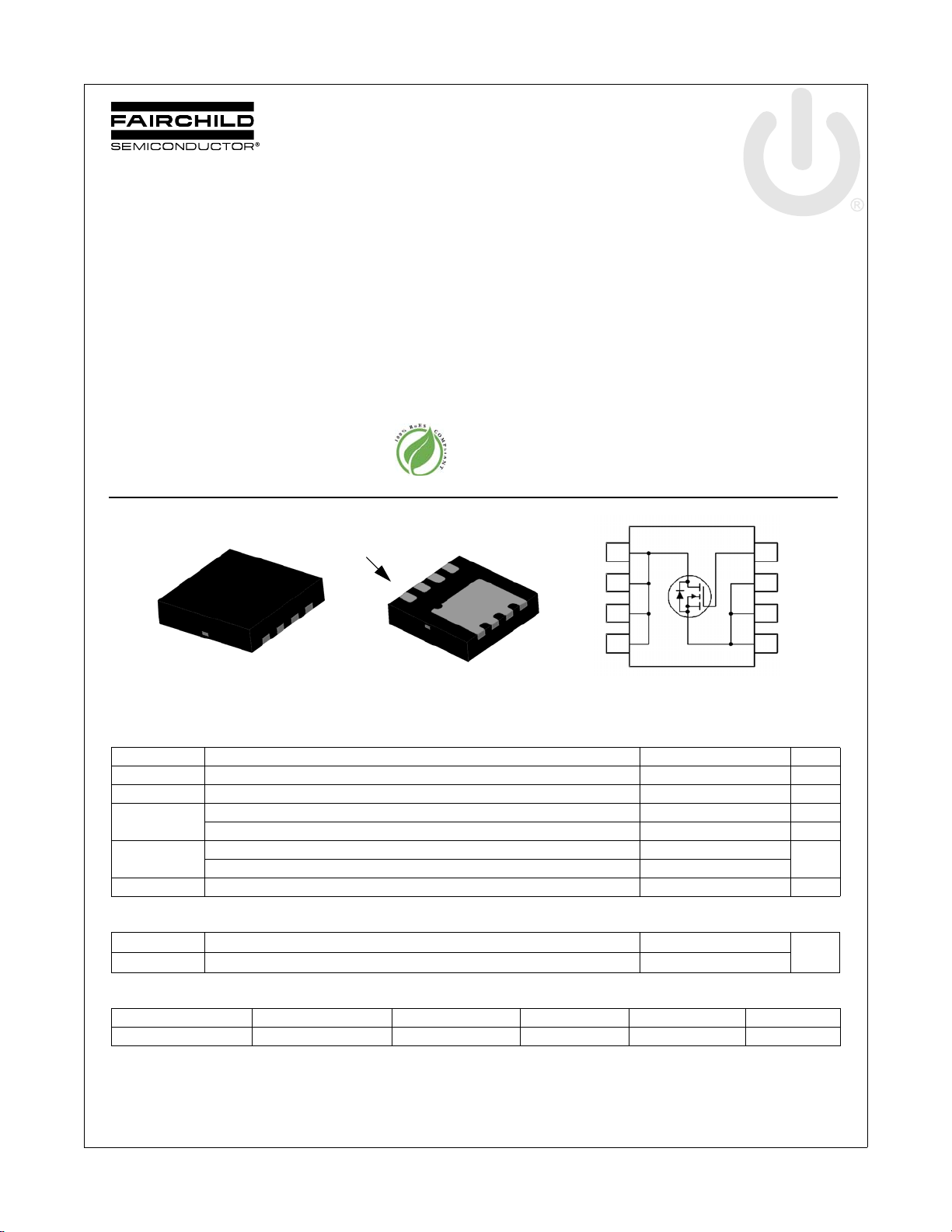
MLP 3.3X3.3
Single N-Channel Logic-Level Power Trench® MOSFET
30 V, 11.5 A, 10.5 mΩ
Features
Max r
Max r
Low Qg, Qgd and Rg for efficient switching performance
RoHS Compliant
= 10.5 mΩ at VGS = 10 V, ID = 11.5 A
DS(on)
= 15 mΩ at VGS = 4.5 V, ID = 10 A
DS(on)
General Description
This single N-Channel MOSFET in the thermally efficient
MicroFET Package has been specifically designed to perform
well in Point of Load converters. Providing an optimized balance
between
used as a “high side” control swtich or “low side” synchronous
rectifier.
r
and gate charge this device can be effectively
DS(on)
FDMC6296 N-Channel Power Trench
November 2010
Application
Point of Load Converters
1/16 Brick Synchronous Rectifier
MOSFET Maximum Ratings T
Symbol Parameter Ratings Units
V
DS
V
GS
I
D
P
D
, T
T
J
STG
Drain to Source Voltage 30 V
Gate to Source Voltage ±20 V
Drain Current -Continuous TA = 25 °C (Note 1a) 11.5 A
-Pulsed 40
Power Dissipation TC = 25 °C 2.1
Power Dissipation T
Operating and Storage Junction Temperature Range -55 to +150 °C
= 25 °C unless otherwise noted
A
= 25 °C (Note 1a) 0.9
A
Thermal Characteristics
®
MOSFET
W
R
θJC
R
θJA
Thermal Resistance, Junction to Case (Note 1) 3
Thermal Resistance, Junction to Ambient (Note 1a) 53
Package Marking and Ordering Information
Device Marking Device Package Reel Size Tape Width Quantity
FDMC6296 FDMC6296 MLP 3.3X3.3 13 ’’ 12 mm 3000 units
©2010 Fairchild Semiconductor Corporation
FDMC6296 Rev. C2
°C/W
1
www.fairchildsemi.com

FDMC6296 N-Channel Power Trench
Electrical Characteristics T
= 25 °C unless otherwise noted
J
Symbol Parameter Test Conditions Min Typ Max Units
Off Characteristics
BV
ΔBV
ΔT
I
DSS
I
GSS
DSS
DSS
J
Drain to Source Breakdown Voltage ID = 250 μA, VGS = 0 V 30 V
Breakdown Voltage Temperature
Coefficient
Zero Gate Voltage Drain Current VDS = 24 V, V
Gate to Source Leakage Current VGS = ±20 V, V
I
= 250 μA, referenced to 25 °C 26 mV/°C
D
= 0 V 1 μA
GS
= 0 V ±100 nA
DS
On Characteristics
V
GS(th)
ΔV
ΔT
r
DS(on)
g
FS
GS(th)
J
Gate to Source Threshold Voltage VGS = VDS, ID = 250 μA11.83V
Gate to Source Threshold Voltage
Temperature Coefficient
Static Drain to Source On Resistance
I
= 250 μA, referenced to 25 °C -6 mV/°C
D
V
= 10 V, ID = 11.5 A 8.7 10.5
GS
= 4.5 V, ID = 10 A 10.6 15
GS
= 10 V , ID = 11.5 A, TJ = 125 °C 13 17
V
GS
Forward Transconductance VDD = 5 V, ID = 11.5 A 49 S
Dynamic Characteristics
C
iss
C
oss
C
rss
R
g
Input Capacitance
Output Capacitance 406 540 pF
Reverse Transfer Capacitance 150 225 pF
Gate Resistance VGS = 0 V, f = 1 MHz 0.9 Ω
Switching Characteristics
t
d(on)
t
r
t
d(off)
t
f
Q
g(TOT)
Q
gs
Q
gd
Turn-On Delay Time
Rise Time 310ns
Turn-Off Delay Time 27 43 ns
Fall Time 816ns
Total Gate Charge at 5V
Total Gate Charge 4nC
Gate to Drain “Miller” Charge 4 nC
= 15 V, VGS = 0 V,
V
DS
f = 1 MHz
= 15 V, ID = 1.0 A,
V
DD
V
= 10 V, R
GS
V
= 5 V
GS
V
= 15 V,
DD
I
= 11.5 A
D
GEN
= 6 Ω
1610 2141 pF
10 20 ns
14 19 nC
mΩV
®
MOSFET
Drain-Source Diode Characteristics
V
SD
t
rr
Q
rr
Notes:
1. R
is determined with the device mounted on a 1in2 pad 2 oz copper pad on a 1.5 x 1.5 in. board o f FR-4 ma teri al. R
θJA
the user's board design.
2. Pulse Test: Pulse Width < 300 μs, Duty cycle < 2.0%.
©2010 Fairchild Semiconductor Corporation
FDMC6296 Rev. C2
Source to Drain Diode Forward Voltage V
Reverse Recovery Time
Reverse Recovery Charge 22 nC
a.
53 °C/W when mounted on a
1 in2 pad of 2 oz copper
= 0 V, IS = 2 A (Note 2) 0.7 1.2 V
GS
= 11.5 A, di/dt = 100 A/μs
I
F
2
θJC
30 ns
is guaranteed by design while R
b.
125 °C/W when mounted on
a minimum pad of 2 oz copper
θCA
is determined by
www.fairchildsemi.com

FDMC6296 N-Channel Power Trench
0.0 0.5 1.0 1.5 2.0
0
10
20
30
40
VGS = 4 V
VGS = 3.5 V
VGS = 4.5 V
PULSE DURA TION = 80 μs
DUTY CYCLE = 0.5% MAX
VGS = 3 V
VGS = 10 V
I
D
, DRAIN CURRENT (A)
V
DS
, DRAIN TO SOURCE VOLTAGE (V)
0 10203040
0
1
2
3
4
5
VGS = 3 V
PULSE DURATION = 80 μs
DUTY CYCLE = 0.5% MAX
NORMALIZED
DRAIN TO SOURCE ON-RESISTANCE
I
D
, DRAIN CURRENT (A)
V
GS
= 4 V
VGS = 4.5 V
VGS = 3.5 V
V
GS
= 10 V
-75 -50 -25 0 25 50 75 100 125 150
0.6
0.8
1.0
1.2
1.4
1.6
1.8
ID = 11.5 A
V
GS
= 10 V
NORMALIZED
DRAIN TO SOURCE ON-RESISTANC E
T
J
, JUNCTION TEMPERATURE (
o
C)
246810
0
20
40
60
TJ = 125 oC
ID = 11.5 A
TJ = 25 oC
V
GS
, GATE TO SOURCE VOLTA G E (V)
r
DS(on)
,
DRAIN TO
SOURCE ON-RESISTANCE
(mΩ)
PULSE DURATION = 80 μs
DUTY CYCLE = 0.5% MAX
012345
0
10
20
30
40
TJ = 125 oC
V
DS
= 5 V
PULSE DURATION = 80 μs
DUTY CYCLE = 0.5% MAX
TJ = -55 oC
TJ = 25 oC
I
D
, DRAIN CURRENT (A)
VGS, GATE TO SOURCE VOLTAGE (V)
0.2 0.4 0.6 0.8 1.0 1.2
0.1
1
10
40
TJ = -55 oC
TJ = 25 oC
TJ = 150 oC
V
GS
= 0 V
I
S
, REVERSE DRAIN CURRENT (A)
VSD, BODY DIODE FORWARD VOLTAGE (V)
Typical Characteristics T
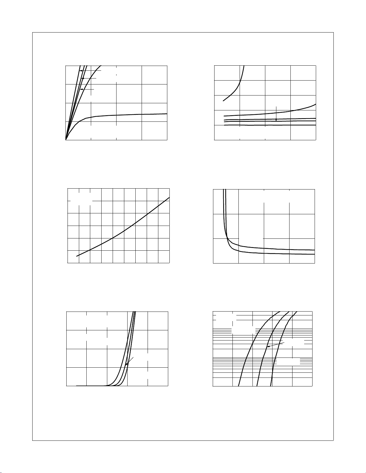
Figure 1.
On Region Characteristics
= 25°C unless otherwise noted
J
Figure 2.
Nor mal ized O n-R esi sta nce
vs Drain Current and Gate Voltage
®
MOSFET
Fi gure 3. N or ma lized On Re si stance
vs Junction Temperature
©2010 Fairchild Semiconductor Corporation
FDMC6296 Rev. C2
Figure 5. Transfer Characteristics
Figure 4.
On-Resistance vs Gate to
Source Voltage
Figure 6.
Source to Drai n Diode
Forward Voltage vs Source Current
3
www.fairchildsemi.com
 Loading...