Fairchild FDMC510P service manual

FDMC510P
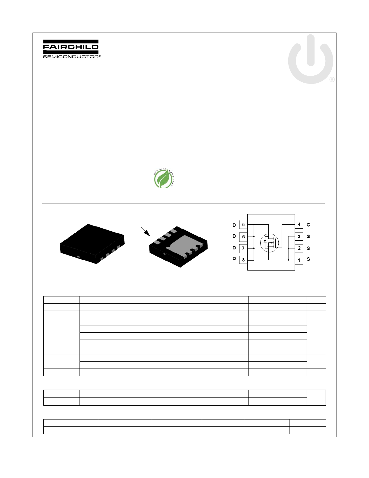
P-Channel PowerTrench® MOSFET
-20 V, -18 A, 8.0 mΩ
Features
Max r
Max r
Max r
Max r
High performance trench technology for extremely low r
High power and current handling capability in a widely used
surface mount package
100% UIL Tested
Termination is Lead-free and RoHS Compliant
HBM ESD capability level >2 KV typical (Note 4)
= 8.0 mΩ at VGS = -4.5 V, ID = -12 A
DS(on)
= 9.8 mΩ at VGS = -2.5 V, ID = -10 A
DS(on)
= 13 mΩ at VGS = -1.8 V, ID = -9.3 A
DS(on)
= 17 mΩ at VGS = -1.5 V, ID = -8.3 A
DS(on)
DS(on)
General Description
This P-Channel MOSFET is produced using Fairchild
Semiconductor’s advanced Power Trench
been
optimized for r
ruggedness.
Applications
Battery Management
Load Switch
®
, switching performance and
DS(ON)
process that has
FDMC510P P-Channel PowerTrench
June 2010
®
MOSFET
Top
Pin 1
S
Bottom
G
S
S
D
D
D
D
MLP 3.3x3.3
MOSFET Maximum Ratings T
Symbol Parameter Ratings Units
V
DS
V
GS
I
D
E
AS
P
D
, T
T
J
STG
Drain to Source Voltage -20 V
Gate to Source Voltage ±8 V
Drain Current -Continuous (Package limited) TC = 25 °C -18
-Continuous (Silicon limited) T
-Continuous T
-Pulsed -50
Single Pulse Avalanche Energy 37 mJ
Power Dissipation TC = 25 °C 41
Power Dissipation T
Operating and Storage Junction Temperature Range -55 to +150 °C
= 25 °C unless otherwise noted
A
= 25 °C -54
C
= 25 °C (Note 1a) -12
A
= 25 °C (Note 1a) 2.3
A
Thermal Characteristics
A
W
R
θJC
R
θJA
Thermal Resistance, Junction to Case 3
Thermal Resistance, Junction to Ambient (Note 1a) 53
Package Marking and Ordering Information
Device Marking Device Package Reel Size Tape Width Quantity
FDMC510P FDMC510P MLP 3.3X3.3 13 ’’ 12 mm 3000 units
©2010 Fairchild Semiconductor Corporation
FDMC510P Rev.C5
°C/W
1
www.fairchildsemi.com

FDMC510P P-Channel PowerTrench
Electrical Characteristics T
= 25 °C unless otherwise noted
J
Symbol Parameter Test Conditions Min Typ Max Units
Off Characteristics
BV
∆BV
∆T
I
DSS
I
GSS
DSS
DSS
J
Drain to Source Breakdown Voltage ID = -250 µA, VGS = 0 V -20 V
Breakdown Voltage Temperature
Coefficient
Zero Gate Voltage Drain Current VDS = -16 V, V
Gate to Source Leakage Current VGS = ±8 V, V
I
= -250 µA, referenced to 25 °C -12 mV/°C
D
= 0 V -1 µA
GS
= 0 V ±100 nA
DS
On Characteristics
V
GS(th)
∆V
∆T
r
DS(on)
g
FS
GS(th)
J
Gate to Source Threshold Voltage VGS = VDS, ID = -250 µA -0.4 -0.5 -1.0 V
Gate to Source Threshold Voltage
Temperature Coefficient
Static Drain to Source On Resistance
I
= -250 µA, referenced to 25 °C 3 mV/°C
D
= -4.5 V, ID = -12 A 6.4 8.0
V
GS
V
= -2.5 V, ID = -10 A 7.6 9.8
GS
= -1.8 V, ID = -9.3 A 9.2 13
V
GS
= -1.5 V, ID = -8.3 A 11 17
V
GS
= -4.5 V, ID = -12 A, TJ = 125 °C 8.5 12
V
GS
Forward Transconductance VDS = -5 V, ID = -12 A 75 S
Dynamic Characteristics
C
iss
C
oss
C
rss
Input Capacitance
Output Capacitance 840 1120 pF
Reverse Transfer Capacitance 738 1110 pF
= -10 V, VGS = 0 V,
V
DS
f = 1 MHz
5910 7860 pF
mΩ
®
MOSFET
Switching Characteristics
t
d(on)
t
r
t
d(off)
t
f
Q
g(TOT)
Q
g(TOT)
Q
gs
Q
gd
Turn-On Delay Time
Rise Time 34 55 ns
Turn-Off Delay Time 338 540 ns
Fall Time 170 272 ns
Total Gate Charge VGS = 0 V to -4.5 V
Total Gate Charge VGS = 0 V to -2.5 V 50 70 nC
Gate to Source Charge 6.3 nC
Gate to Drain “Miller” Charge 20.4 nC
= -10 V, ID = -12 A,
V
DD
V
= -4.5 V, R
GS
GEN
= 6 Ω
Drain-Source Diode Characteristics
V
= 0 V, IS = -12 A (Note 2) -0.70 -1.3
V
SD
t
rr
Q
rr
Notes:
1: R
θJA
by the user’s board design.
Source to Drain Diode Forward Voltage
Reverse Recovery Time
Reverse Recovery Charge 20 32 nC
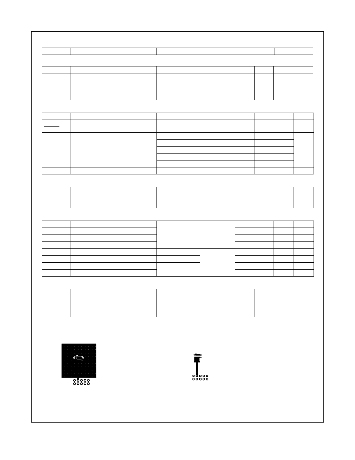
is determined with the device mounted on a 1 in2 pad 2 oz copper pad on a 1.5 x 1.5 in. board of FR-4 material. R
a. 53 °C/W when mounted on
a 1 in2 pad of 2 oz c o p p e r
GS
= 0 V, IS = -2 A (Note 2) -0.53 -1.2
V
GS
= -12 A, di/dt = 100 A/µs
I
F
= -10 V,
V
DD
I
= -12 A
D
15 27 ns
83 116 nC
35 57 ns
is guaranteed by design while R
θJC
b. 125 °C/W when mounted on a
minimum pad of 2 oz copper
V
is determined
θJA
2: Pulse Test: Pulse Width < 300 µs, Duty cycle < 2.0%.
3: Starting T
4: No gate overvoltage rating is implied.
FDMC510P Rev.C5
= 25oC; P-Ch: L = 3 mH, IAS = -5 A, VDD = -20 V, VGS = -4.5 V.
J
2
www.fairchildsemi.com

FDMC510P P-Channel PowerTrench
Typical Characteristics T
50
40
30
20
DRAIN CURRENT (A)
,
D
10
-I
0
0.0 0.5 1.0 1.5 2.0
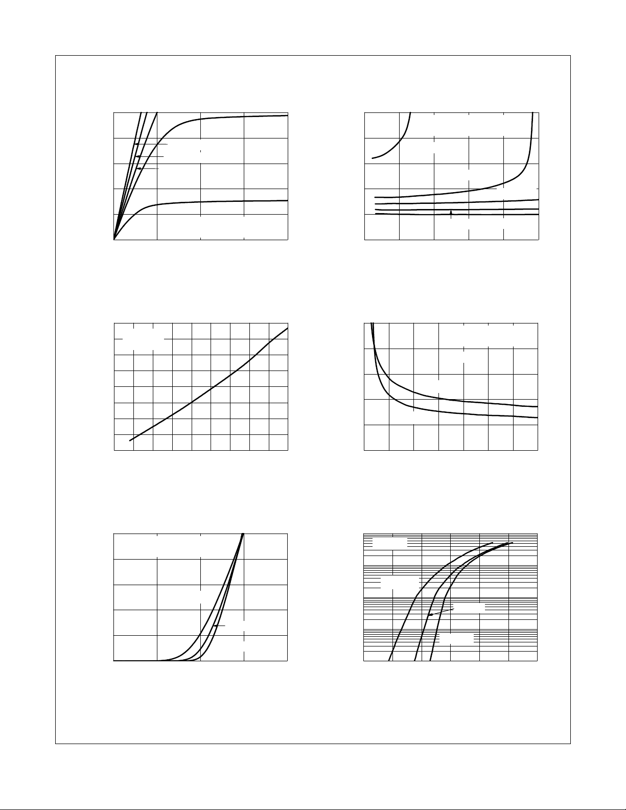
Figure 1.
1.5
ID = -12 A
NORMALIZED
DRAIN TO SOURCE ON-RESISTANCE
1.4
1.3
1.2
1.1
1.0
0.9
0.8
0.7
= -4.5 V
V
GS
-75 -50 -25 0 25 50 75 100 125 150
VGS = -4.5 V
VGS = -2.5 V
VGS = -1.8 V
PULSE DURATION = 80 µs
DUTY CYCLE = 0.5%MAX
-V
,
DRAIN TO SOURCE VOLTAGE (V)
DS
On Region Characteristics Figure 2.
T
,
JUNCTION TEMPERATUR E
J
= 25 °C unless otherwise noted
J
VGS = - 1.5 V
VGS = -1.2 V
o
(
C
)
5
PULSE DURATION = 80 µs
4
DUTY CYCLE = 0.5%MAX
VGS = -1.2 V
3
2
NORMALIZED
VGS = -1.5 V
VGS = -1.8 V
1
V
= -2.5 V
DRAIN TO SOURCE ON-RESISTANCE
0
0 1020304050
-I
D
GS
,
DRAIN CURRENT (A)
V
GS
Normalized On-Resistance
vs Drain Current and Gate Voltage
25
)
Ω
20
m
(
15
10
, DRAIN TO
DS(on)
r
5
SOURCE ON-RESISTANCE
0
1.0 1.5 2.0 2.5 3.0 3.5 4.0 4.5
T
= 25 oC
J
-V
,
GATE TO S OURCE VO LTAGE (V
GS
PULSE DURATION = 80 µs
DUTY CYCLE = 0.5%MAX
ID = -12 A
TJ = 125 oC
)
= -4.5 V
®
MOSFET
Fi g ure 3 . Norma l i zed O n Resi s t ance
50
40
30
20
, DRAIN CURRENT (A)
D
10
-I
0
0.0 0.5 1.0 1.5 2.0
FDMC510P Rev.C5
vs Junction Temperature
PULSE DURATION = 80 µs
DUTY CYCLE = 0.5%MAX
V
= -5 V
DS
TJ = 150 oC
TJ = 25 oC
TJ = -55 oC
-VGS, GATE TO SOURCE VO LTAGE (V)
Figure 5. Transfer Characteristics
Figure 4.
On-Resi st an ce vs Gate to
Source Voltage
100
V
= 0 V
GS
10
TJ = 150 oC
1
TJ = 25 oC
0.1
, REVERSE DRAIN CURRENT (A)
S
-I
0.01
0.00.20.40.60.81.01.2
-VSD, BODY DIODE FORWARD VOLTAGE (V)
Figure 6.
Sou rc e t o D rain Di ode
TJ = -55 oC
Forward Voltage vs Source Current
3
www.fairchildsemi.com
 Loading...