

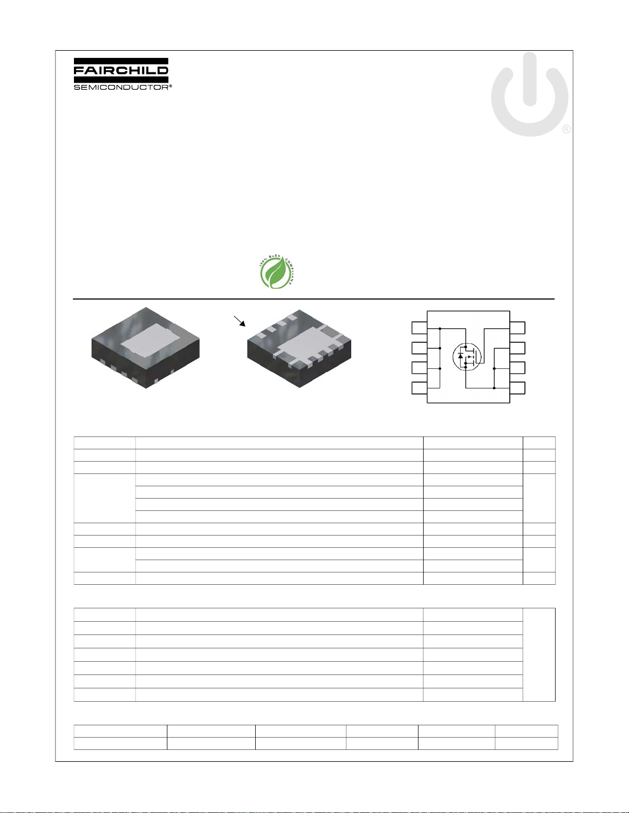
FDMC3020DC
N-Channel Dual CoolTM PowerTrench® MOSFET
30 V, 40 A, 6.25 mΩ
Features
Dual CoolTM Top Side Cooling PQFN package
Max r
Max r
High performance technology for extremely low r
RoHS Compliant
= 6.25 mΩ at VGS = 10 V, ID = 12 A
DS(on)
= 9.0 mΩ at VGS = 4.5 V, ID = 10 A
DS(on)
DS(on)
General Description
This N-Channel MOSFET is produced using Fairchild
Semiconductor’s advanced PowerTrench
Advancements in both silicon and Dual Cool
technologies have been combined to offer the lowest r
while maintaining excellent switching performance by extremely
low Junction-to-Ambient thermal resistance.
Applications
Synchronous Rectifier for DC/DC Converters
Telecom Secondary Side Rectification
High End Server/Workstation
July 2012
®
process.
TM
package
DS(on)
FDMC3020DC N-Channel Dual Cool
TM
PowerTrench
Pin 1
S
Top
MOSFET Maximum Ratings T
Symbol Parameter Ratings Units
V
DS
V
GS
I
D
E
AS
dv/dt Peak Diode Recovery dv/dt (Note 4) 1.6 V/ns
P
D
, T
T
J
STG
Drain to Source Voltage 30 V
Gate to Source Voltage ±20 V
Drain Current -Continuous (Package limited) TC = 25 °C 40
-Continuous (Silicon limited) T
-Continuous T
-Pulsed 100
Single Pulse Avalanche Energy (Note 3) 60 mJ
Power Dissipation TC = 25 °C 50
Power Dissipation T
Operating and Storage Junction Temperature Range -55 to +150 °C
Power 33
A
G
S
S
D
D
D
D
Bottom
= 25°C unless otherwise noted
= 25 °C 70
C
= 25 °C (Note 1a) 17
A
= 25 °C (Note 1a) 3.0
A
G
5
D
D
6
D
7
8
D
4
S
3
S
2
S
1
W
Thermal Characteristics
®
MOSFET
A
R
θJC
R
θJC
R
θJA
R
θJA
R
θJA
R
θJA
R
θJA
Thermal Resistance, Junction to Case (Top Source) 7.9
Thermal Resistance, Junction to Case (Bottom Drain) 2.5
Thermal Resistance, Junction to Ambient (Note 1a) 42
Thermal Resistance, Junction to Ambient (Note 1b) 105
Thermal Resistance, Junction to Ambient (Note 1i) 17
Thermal Resistance, Junction to Ambient (Note 1j) 26
Thermal Resistance, Junction to Ambient (Note 1k) 12
Package Marking and Ordering Information
Device Marking Device Package Reel Size Tape Width Quantity
3020 FDMC3020DC Dual Cool
©2012 Fairchild Semiconductor Corporation
FDMC3020DC Rev.C4
TM
Power 33 13’’ 12 mm 3000 units
1
www.fairchildsemi.com
°C/W
FDMC3020DC N-Channel Dual Cool
Electrical Characteristics T
= 25 °C unless otherwise noted
J
Symbol Parameter Test Conditions Min Typ Max Units
Off Characteristics
BV
ΔBV
ΔT
I
DSS
I
GSS
DSS
DSS
J
Drain to Source Breakdown Voltage ID = 250 μA, VGS = 0 V 30 V
Breakdown Voltage Temperature
Coefficient
Zero Gate Voltage Drain Current VDS = 24 V, V
Gate to Source Leakage Current VGS = ±20 V, V
= 250 μA, referenced to 25 °C 17 mV/°C
I
D
= 0 V 1 μA
GS
= 0 V ±100 nA
DS
On Characteristics
V
GS(th)
ΔV
ΔT
r
DS(on)
g
FS
GS(th)
J
Gate to Source Threshold Voltage VGS = VDS, ID = 250 μA 1.0 1.9 3.0 V
Gate to Source Threshold Voltage
Temperature Coefficient
Static Drain to Source On Resistance
I
= 250 μA, referenced to 25 °C -6 mV/°C
D
= 10 V, ID = 12 A 5.0 6.25
V
GS
= 4.5 V, ID = 10 A 7.2 9.0
GS
= 10 V, ID = 12 A, TJ = 125 °C 7.5 9.1
V
GS
Forward Transconductance VDS = 5 V, ID = 12 A 44 S
Dynamic Characteristics
C
iss
C
oss
C
rss
R
g
Input Capacitance
Output Capacitance 513 685 pF
Reverse Transfer Capacitance 87 135 pF
= 15 V, VGS = 0 V,
V
DS
f = 1 MHz
Gate Resistance 0.9 Ω
1038 1385 pF
0.1 2.0
Switching Characteristics
t
d(on)
t
r
t
d(off)
t
f
Q
Q
Q
Q
Turn-On Delay Time
Rise Time 310ns
Turn-Off Delay Time 19 35 ns
= 15 V, ID = 12 A,
V
DD
V
= 10 V, R
GS
GEN
= 6 Ω
Fall Time 210ns
g
g
gs
gd
Total Gate Charge VGS = 0 V to 10 V
Total Gate Charge VGS = 0 V to 4.5 V 7.1 10.6 nC
Gate to Source Gate Charge 3 nC
V
DD
I
= 12 A
D
= 15 V,
Gate to Drain “Miller” Charge 2.5 nC
918ns
15.5 23 nC
mΩV
TM
PowerTrench
®
MOSFET
Drain-Source Diode Characteristics
V
SD
t
rr
Q
rr
©2012 Fairchild Semiconductor Corporation
FDMC3020DC Rev.C4
Source to Drain Diode Forward Voltage
Reverse Recovery Time
Reverse Recovery Charge 9 18 nC
V
= 0 V, IS = 12 A (Note 2) 0.82 1.3
GS
= 0 V, IS = 1.9 A (Note 2) 0.73 1.2
V
GS
= 12 A, di/dt = 100 A/μs
I
F
2
25 45 ns
V
www.fairchildsemi.com
Thermal Characteristics
FDMC3020DC N-Channel Dual Cool
R
θJC
R
θJC
R
θJA
R
θJA
R
θJA
R
θJA
R
θJA
R
θJA
R
θJA
R
θJA
R
θJA
R
θJA
R
θJA
R
θJA
NOTES:
is determined with the device mounted on a FR-4 board using a specified pad of 2 oz copper as shown below. R
1. R
θJA
by the user's board design.
Thermal Resistance, Junction to Case (Top Source) 7.9
Thermal Resistance, Junction to Case (Bottom Drain) 2.5
Thermal Resistance, Junction to Ambient (Note 1a) 42
Thermal Resistance, Junction to Ambient (Note 1b) 105
Thermal Resistance, Junction to Ambient (Note 1c) 29
Thermal Resistance, Junction to Ambient (Note 1d) 40
Thermal Resistance, Junction to Ambient (Note 1e) 19
Thermal Resistance, Junction to Ambient (Note 1f) 23
Thermal Resistance, Junction to Ambient (Note 1g) 30
Thermal Resistance, Junction to Ambient (Note 1h) 79
Thermal Resistance, Junction to Ambient (Note 1i) 17
Thermal Resistance, Junction to Ambient (Note 1j) 26
Thermal Resistance, Junction to Ambient (Note 1k) 12
Thermal Resistance, Junction to Ambient (Note 1l) 16
a. 42 °C/W when mounted on
a 1 in2 pa d of 2 oz c opp er
is guaranteed by design while R
θJC
b. 105 °C/W when mounted on
a minimum pad of 2 oz copper
is determined
θCA
°C/W
TM
PowerTrench
®
MOSFET
c. Still air, 20.9x10.4x12.7mm Aluminum Heat Sink, 1 in
d. Still air, 20.9x10.4x12.7mm Aluminum Heat Sink, minimum pad of 2 oz copper
e. Still air, 45.2x41.4x11.7mm Aavid Thermalloy Part # 10-L41B-11 Heat Sink, 1 in2 pad of 2 oz copper
f. Still air, 45.2x41.4x11.7mm Aavid Thermalloy Part # 10-L41B-11 Heat Sink, minimum pad of 2 oz copper
g. 200FPM Airflow, No Heat Sink,1 in2 pad of 2 oz copper
h. 200FPM Airflow, No Heat Sink, minimum pad of 2 oz copper
i. 200FPM Airflow, 20.9x10.4x12.7mm Aluminum Heat Sink, 1 in
j. 200FPM Airflow, 20.9x10.4x12.7mm Aluminum Heat Sink, minimum pad of 2 oz copper
k. 200FPM Airflow, 45.2x41.4x11.7mm Aavid Thermalloy Part # 10-L41B-11 Heat Sink, 1 in2 pad of 2 oz copper
l. 200FPM Airflow, 45.2x41.4x11.7mm Aavid Thermalloy Part # 10-L41B-11 Heat Sink, minimum pad of 2 oz copper
2. Pulse Test: Pulse Width < 300 μs, Duty cycle < 2.0%.
3. EAS of 60 mJ is based on starting TJ = 25 °C, L = 1 mH, IAS = 11 A, VDD = 27 V, VGS = 10 V.
4. ISD ≤ 12 A, di/dt ≤ 100 A/μs, VDD ≤ BV
©2012 Fairchild Semiconductor Corporation
FDMC3020DC Rev.C4
, Starting TJ = 25 oC.
DSS
2
pad of 2 oz copper
2
pad of 2 oz copper
3
www.fairchildsemi.com

FDMC3020DC N-Channel Dual Cool
Typical Characteristics
50
VGS = 10V
40
30
20
DRAIN CURRENT (A)
,
10
D
I
0
012345
Figure 1.
1.8
ID = 12A
V
1.6
1.4
1.2
1.0
NORMALIZED
O SOURCE ON-RESISTANCE
0.8
DRAIN T
0.6
-50 -25 0 25 50 75 10
F i g u r e 3 . N o r m a l i z e d O n - R e s i s t a n c e
VGS = 4.5V
VGS = 4V
PULSE DURATION = 8
DUTY CYCLE = 0.5
,
V
DRAIN TO SOURCE VOLTAGE (V
DS
On-Region Characteristics Figure 2.
= 10V
GS
,
T
JUNCTION TEMPE
J
vs Junction Temperature
TJ = 25°C unless otherwise noted
VGS = 3.5V
0
s
P
%MAX
VGS = 3V
)
0 125 150
o
(
RATURE
)
C
6
P
PULSE DURATION =
5
DUTY CYCLE = 0.5%MAX
VGS = 3V
80
s
4
VGS = 3.5V
V
V
= 4V
GS
GS
= 4.5V
NORMALIZED
3
2
1
V
=10V
DRAIN TO SOURCE ON-RESISTANCE
0
0 1020304050
DRAIN CURRENT(A)
I
,
D
N o r m a l i z e d O
n - R e s i s t a n c e
GS
vs Drain Current and Gate Voltage
50
)
:
m
40
(
E
30
DRAIN TO
,
20
DS(on)
r
10
SOURCE ON-RESISTANC
0
TJ= 25oC
246810
V
GS
Figure
O n - R es i s t a
4.
PULSE DURATION =
DUTY CYCLE = 0.5%MAX
ID= 12A
TJ= 125oC
,
GATE TO SOURCE VOL
n c e v s G a t e t o
80
TAGE (V)
s
P
Source Voltage
TM
Power Trench
®
MOSFET
50
PULSE DURATION = 8
DUTY CYCLE = 0.5%MAX
40
VDS= 5V
30
20
TJ= 150oC
, DRAIN CURRENT (A)
10
D
I
0
12345
VGS, GATE TO SOURCE V
Figure 5. Transfer Characteristics
©2012 Fairchild Semiconductor Corporation
FDMC3020DC Rev.C4
0
s
P
TJ= 25oC
TJ= -55oC
OLTAGE (V)
50
V
= 0V
GS
10
1
TJ= 150oC
TJ = 25oC
0.1
1
0.0
, REVERSE DRAIN CURRENT (A)
S
I
0.001
0.0 0.2 0.4 0.6 0.8 1.0 1.2
VSD, BODY DIODE FORWA
Figure 6.
S o u r ce t o D
TJ = -55oC
RD VOLTAGE (V)
r a i n Di o d e
Forward Voltage vs Source Current
4
www.fairchildsemi.com

FDMC3020DC N-Channel Dual Cool
Typical Characteristics
10
ID= 12A
(V)
8
6
4
2
, GATE TO SOURCE VOLTAGE
GS
V
0
0 3 6 9 12 15 18
Figure 7.
Gate Charge Characteristics Figure 8.
30
10
, AVALANCHE CURRENT(A)
AS
I
1
0.01 0.1 1 10 100
tAV, TI ME IN AVALANCHE(m
Figure 9.
Switching Capability
V
= 10V
DD
Qg, GATE CHARGE(nC)
TJ= 125oC
U n c l a m p e d I n d u c t i
TJ = 25°C unless otherwise noted
VDD = 15V
VDD = 20V
TJ= 25oC
s)
v e
3000
C
1000
100
CAPACITANCE (pF)
f = 1MHz
V
= 0V
GS
30
0.1 1 10 30
VDS, DRAIN TO SOURCE VOLTAGE (V
iss
C
oss
C
rss
)
C a p a c i t a n c e v s D r a i n
to Source Voltage
80
R
= 2.5 oC/W
V
= 10 V
GS
θJC
60
V
= 4.5 V
GS
40
Limited by Package
, DRAIN CURRENT (A)
20
D
I
0
25 50 75 100 125 150
T
, CASE TEMPERATURE (
C
o
C)
Figure 10. M a x i m u m C o n t i n u o u s D r a i n
C u r r e n t v s C a s e T e m p e r a t ur e
TM
Power Trench
®
MOSFET
300
100
10
1
THIS AREA IS
LIMITED BY r
0.1
SINGLE PULSE
= MAX RATED
T
, DRAIN CURRENT (A)
D
I
0.001
J
R
0.01
θJA
T
A
0.01 0.1 1 10 100200
Figure 11.
DS(on)
o
= 105
C/W
o
= 25
C
VDS, DRAIN to SOURCE VOLTAGE ( V)
Forward Bi as Sa fe
Operating Area
©2012 Fairchild Semiconductor Corporation
FDMC3020DC Rev.C4
2000
1000
100 us
1ms
10 ms
100 ms
1 s
10 s
DC
100
10
, PEAK TRANSIENT POWER (W)
1
(PK)
P
0.5
10-410-310-210
-1
t, PULSE WIDTH (sec)
SINGLE PULSE
R
T
A
110
= 105 oC/W
θJA
= 25 oC
100 1000
Figure 12. S i n g l e P u l s e M a x i m u m
Power Dissipation
5
www.fairchildsemi.com

FDMC3020DC N-Channel Dual Cool
Typical Characteristics
2
DUTY CYCLE-DESCENDING ORDER
1
D = 0.5
0.2
0.1
0.01
10
0.1
0.05
0.02
0.01
-4
-3
10
Figure 13. Junction-to-Ambient Transient Thermal Response Curve
NORMALIZED THERMAL
θJA
Z
IMPEDANCE,
0.001
0.0005
TJ = 25°C unless otherwise noted
SINGLE PULSE
R
= 105 oC/W
θJA
-2
10
t, RECTANGULAR PULSE DURATION (sec)
-1
10
P
DM
NOTES:
DUTY FACTOR: D = t1/t
PEAK TJ = PDM x Z
θJA
x R
110
t
1
t
2
2
+ T
θJA
A
100 1000
TM
Power Trench
®
MOSFET
©2012 Fairchild Semiconductor Corporation
FDMC3020DC Rev.C4
6
www.fairchildsemi.com
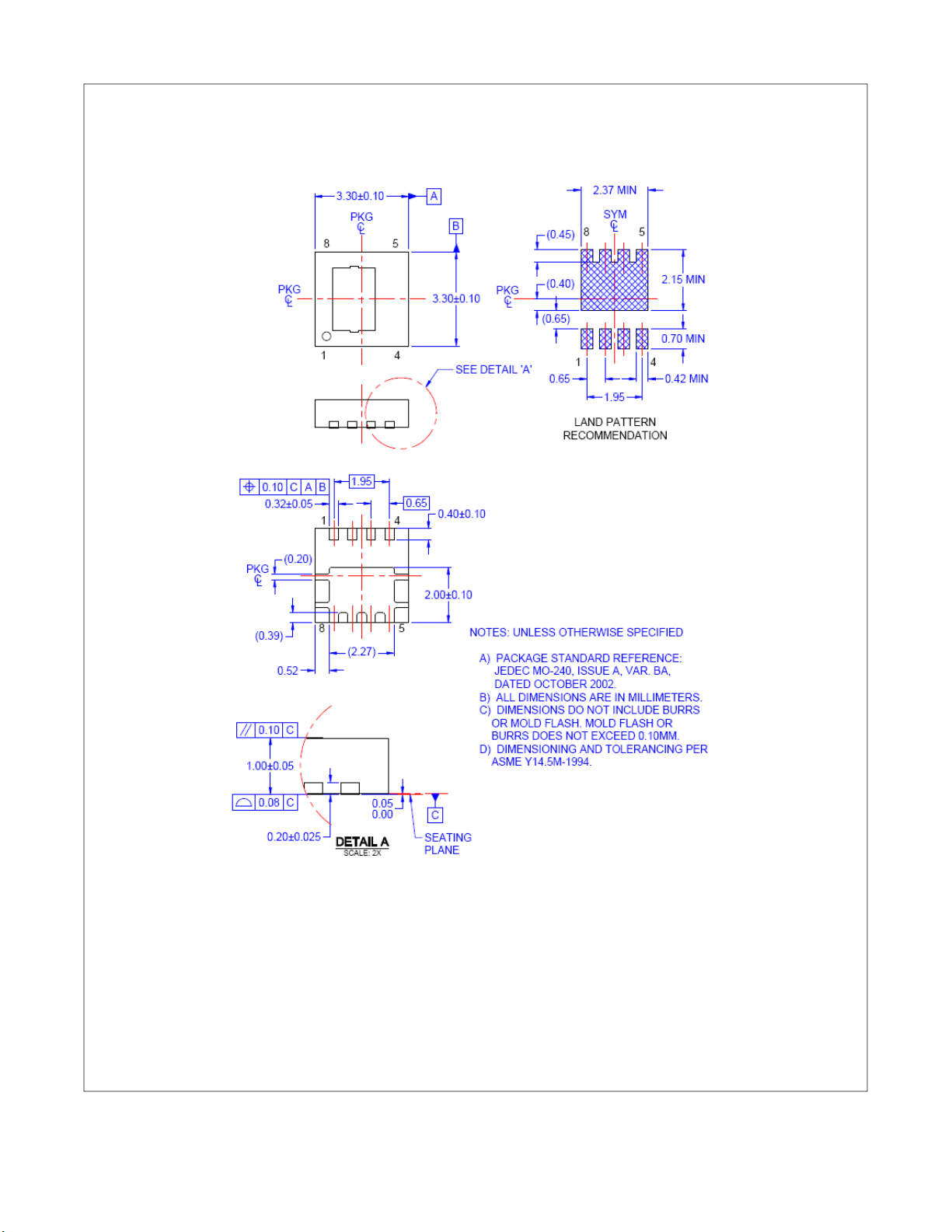
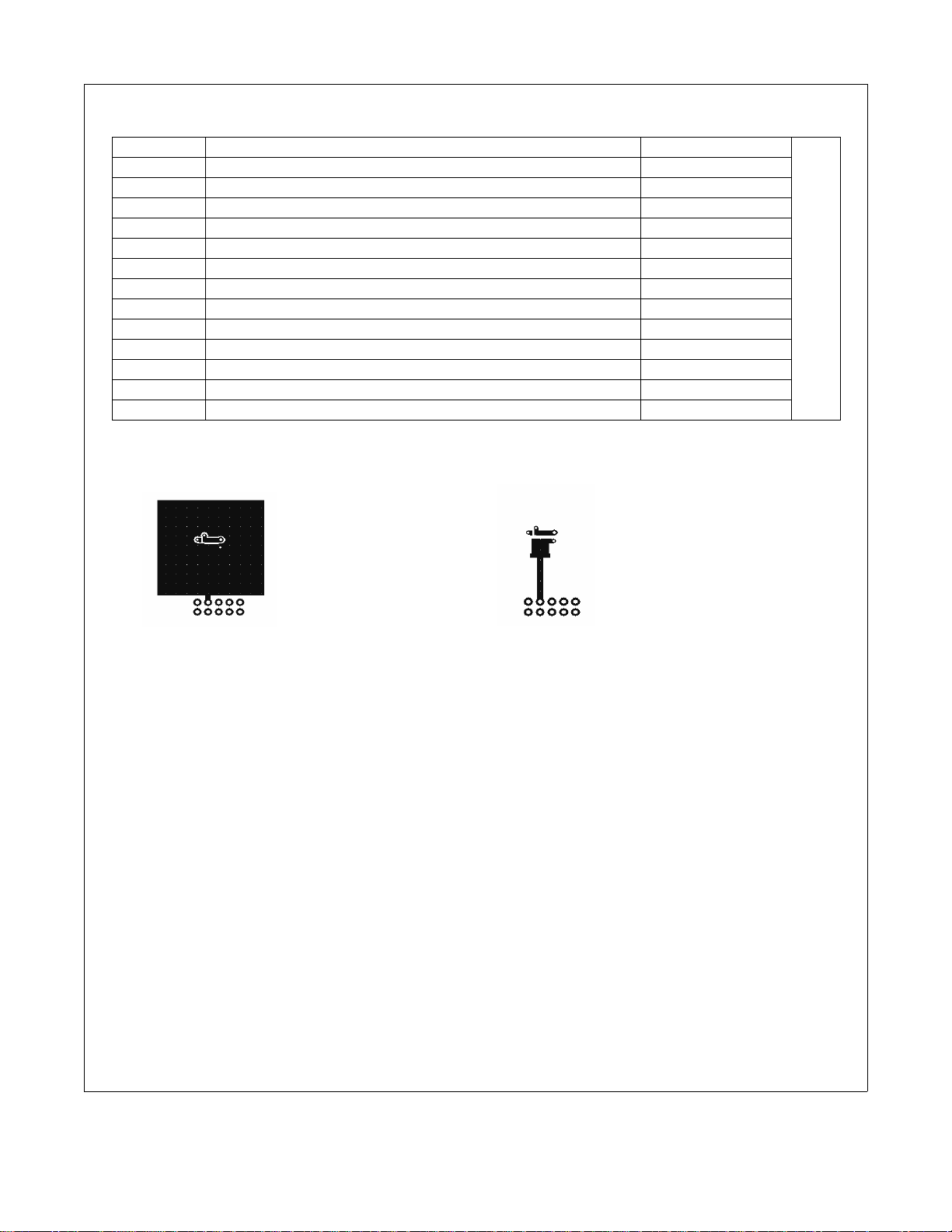
Dimensional Outline and Pad Layout
FDMC3020DC N-Channel Dual Cool
TM
PowerTrench
®
MOSFET
©2012 Fairchild Semiconductor Corporation
FDMC3020DC Rev.C4
7
www.fairchildsemi.com

®
™
tm
tm
TRADEMARKS
The following includes registered and unregistered trademarks a nd service marks, owned by Fairch ild Semiconductor and/or its global subsidiaries, and is n ot
intended to be an exhaustive list of all such trademarks.
2Cool™
AccuPower™
AX-CAP™*
®
BitSiC
Build it Now™
CorePLUS™
CorePOWER™
CROSSVOLT™
CTL™
Current Transfer Logic™
DEUXPEED
Dual Cool™
EcoSPARK
EfficentMax™
®
®
ESBC™
®
Fairchild
Fairchild Semiconductor
FACT Quiet Series™
®
FACT
®
FAST
FastvCore™
FETBench™
FlashWriter
®
*
FPS™
F-PFS™
®
FRFET
Global Power Resource
Green Bridge™
Green FPS™
Green FPS™ e-Series™
Gmax™
GTO™
IntelliMAX™
ISOPLANAR™
Marking Small Speakers Sound Louder
and Better™
MegaBuck™
MICROCOUPLER™
MicroFET™
MicroPak™
MicroPak2™
®
MillerDrive™
MotionMax™
Motion-SPM™
mWSaver™
OptoHiT™
OPTOLOGIC
®
OPTOPLANAR
®
SM
®
PowerTrench
PowerXS™
Programmable Active Droop™
QFET
QS™
Quiet Series™
RapidConfigure™
Saving our world, 1mW/W/kW at a time™
SignalWise™
SmartMax™
SMART START™
Solutions for Your Success™
SPM
STEALTH™
SuperFET
SuperSOT™-3
SuperSOT™-6
SuperSOT™-8
SupreMOS
SyncFET™
Sync-Lock™
*Trademarks of System General Corporation, used under license by Fairchild Semiconductor.
DISCLAIMER
FAIRCHILD SEMICONDUCTOR RESERVES THE RIGHT TO MAKE CHANGES WITHOUT FURTHER NOTICE TO ANY PRODUCTS HEREIN TO IMPROVE
RELIABILITY, FUNCTION, OR DESIGN. FAIRCHILD DOES NOT ASSUME ANY LIABILITY ARISING OUT OF THE APPLICATION OR USE OF ANY
PRODUCT OR CIRCUIT DESCRIBED HEREIN; NEITHER DOES IT CONVEY ANY LICENSE UNDER ITS PATENT RIGHTS, NOR THE RIGHTS OF OTHERS.
THESE SPECIFICATIONS DO NOT EXPAND THE TERMS OF FAIRCHILD’S WORLDWIDE TERMS AND CONDITIONS, SPECIFICALLY THE WARRANTY
THEREIN, WHICH COVERS THESE PRODUCTS.
®
®
®
®
®
®*
The Power Franchise
TinyBoost™
TinyBuck™
TinyCalc™
®
TinyLogic
TINYOPTO™
TinyPower™
TinyPWM™
TinyWire™
®
TranSiC
TriFault Detect™
TRUECURRENT
μSerDes™
®
UHC
Ultra FRFET™
UniFET™
VCX™
VisualMax™
VoltagePlus™
XS™
®
®
®
*
FDMC3020DC N-Channel Dual Cool
TM
PowerTrench
®
MOSFET
LIFE SUPPORT POLICY
FAIRCHILD’S PRODUCTS ARE NOT AUTHORIZED FOR USE AS CRITICAL COMPONENTS IN LIFE SUPPORT DEVICES OR SYSTEMS WITHOUT THE
EXPRESS WRITTEN APPROVAL OF FAIRCHILD SEMICONDUCTOR CORPORATION.
As used here in:
1. Life support devices or systems are devices or systems which, (a) are
intended for surgical implant into the bo dy or (b ) support or sustain life,
and (c) whose failure to perform when properly used in accordan ce with
instructions for use provided in the labeling, can be reasonably
2. A critical component in any component of a life support, device, or
system whose failure to perform can be reasonably expected to cause
the failure of the life support device or system, or to affect its safety or
effectiveness.
expected to result in a significant injury of the user.
ANTI-COUNTERFEITING POLICY
Fairchild Semiconductor Corporation’s Anti-Counterfeiting Policy. Fairchild’s Anti-Counterfeiting Policy is also stated on our external website,
www.Fairchildsemi.com, under Sales Support
Counterfeiting of semiconductor parts is a growing problem in the industry. All manufactures of semiconductor products are exper iencing counterfeiting of their
parts. Customers who inadvertently purchase counterfeit part s expe rience many problems such as loss of brand repu tatio n, substandar d pe rformance, f ail ed
application, and increased cost of production and manufacturing delays. Fairchild is taki ng st ron g measures to prote ct ourselves and our custo mers from the
proliferation of counterfeit parts. Fairchild strongl y encourages customers t o purchase Fairchil d parts either d irectly from Fairchild o r from Authorized Fairchild
Distributors who are listed by country on our web page cited above. Products customers buy either from Fairchild directly or from Authorized Fairchild
Distributors are genuine parts, have full traceability, me et Fairchild’s quality standards for handing and storage and provide access to Fairchild’s full range of
up-to-date technical and product information. Fairchild and our Authorized Distributors will stand behind all warranties and will appropriately address and
warranty issues that may arise. Fairchild will not provide any warranty coverage or other assistance for parts bought from Unauthorized Sources. Fairchild is
committed to combat this global problem and encourage our customers to do their part in stopping this practi ce by buying direct or fr om authorized distributors.
PRODUCT STATUS DEFINITIONS
Definition of Terms
.
Datasheet Identification Product Status Definition
Advance Information Formative / In Design
Preliminary First Production
No Identification Needed Full Production
Obsolete Not In Production
Datasheet contains the design specifications for product development. Specifications
may change in any manner without notice.
Datasheet contains preliminary data; supplementary data will be published at a later
date. Fairchild Semiconductor reserves the right to make changes at any time without
notice to improve design.
Datasheet contains final specifications. Fairchild Semiconductor re serves the right to
make changes at any time without notice to improve the design.
Datasheet contains specifications on a product that is discontinued by Fairchild
Semiconductor. The data sh eet is for reference information only.
Rev. I61
©2012 Fairchild Semiconductor Corporation
FDMC3020DC Rev.C4
8
www.fairchildsemi.com
 Loading...