tm
FDMC2674
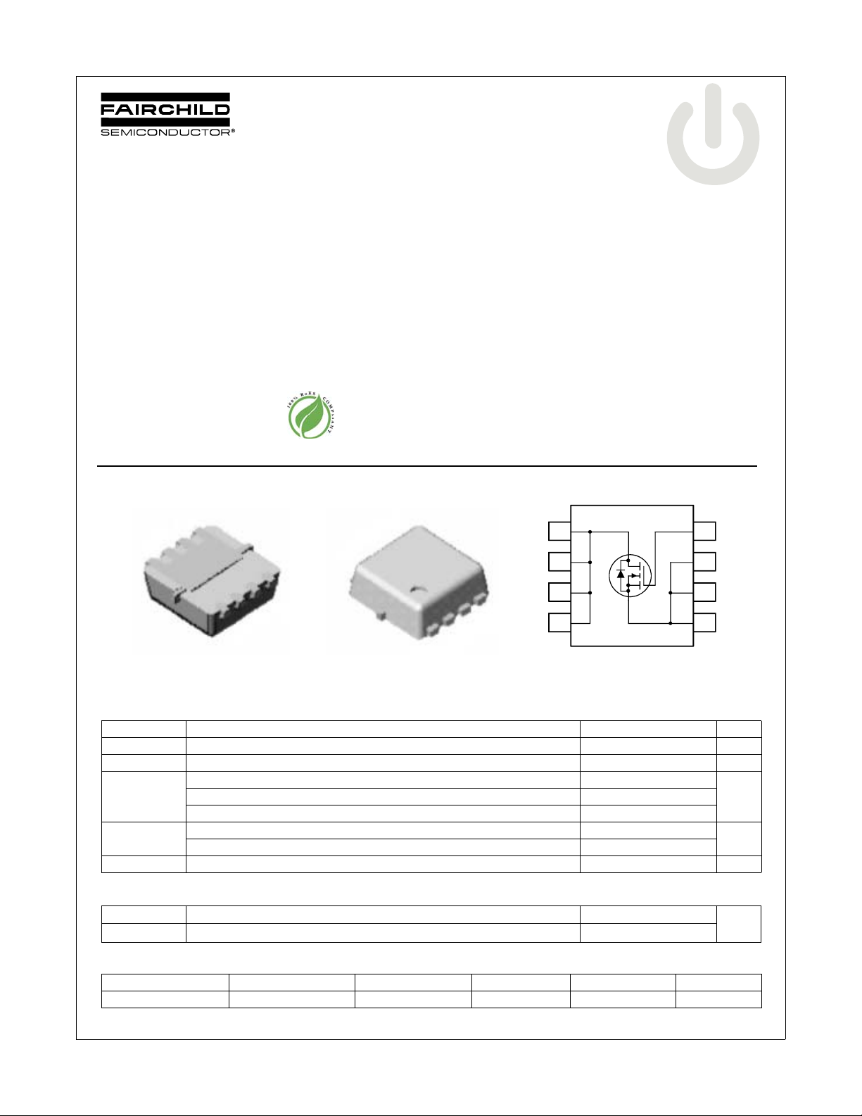
N-Channel UltraFET Trench MOSFET
220V, 7.0A, 366mΩ
Features
Max r
Typ Qg = 12.7nC at VGS = 10V
Low Miller charge
Low Qrr Body Diode
Optimized efficiency at high frequencies
UIS Capability ( Single Pulse and Repetitive Pulse)
RoHS Compliant
= 366mΩ at VGS = 10V, ID = 1.0A
DS(on)
General Description
UltraFET device combines characteristics that enable
benchmark efficiency in power conversion applications.
Optimized for r
these devices are ideal for high frequency DC to DC converters.
DS(on)
Application
DC/DC converters and Off-Line UPS
Distributed Power Architectures
FDMC2674 N-Channel UltraFET Trench MOSFET
January 2007
, low ESR, low total and Miller gate charge,
Bottom
8
7
6
5
1
2
3
4
D
D
Top
D
D
G
S
S
S
D
5
D
6
D
7
D
8
Power 33
MOSFET Maximum Ratings T
Symbol Parameter Ratings Units
V
DS
V
GS
I
D
P
D
, T
T
J
STG
Drain to Source Voltage 220 V
Gate to Source Voltage ±20 V
Drain Current -Continuous (Silicon limited) TC= 25°C 7.0
-Pulsed 13.8
Power Dissipation TC = 25°C 42
Power Dissipation T
Operating and Storage Junction Temperature Range -55 to +150 °C
= 25°C unless otherwise noted
A
= 25°C (Note 1b) 1.0
A
= 25°C (Note 1a) 2.1
A
Thermal Characteristics
G
4
S
3
S
2
S
1
A -Continuous T
W
R
θJC
R
θJA
Thermal Resistance, Junction to Case (Note 1) 3.0
Thermal Resistance, Junction to Ambient (Note 1a) 60
Package Marking and Ordering Information
Device Marking Device Package Reel Size Tape Width Quantity
FDMC2674 FDMC2674 Power 33 7’’ 8mm 3000 units
©2006 Fairchild Semiconductor Corporation
FDMC2674 Rev.F
°C/W
1
www.fairchildsemi.com

FDMC2674 N-Channel UltraFET Trench MOSFET
Electrical Characteristics T
= 25°C unless otherwise noted
J
Symbol Parameter Test Conditions Min Typ Max Units
Off Characteristics
BV
DSS
ΔBV
DSS
ΔT
J
I
DSS
I
GSS
On Characteristics
V
GS(th)
ΔV
GS(th)
ΔT
J
r
DS(on)
Drain to Source Breakdown Voltage ID = 250μA, VGS = 0V 220 V
Breakdown Voltage Temperature
Coefficient
ID = 250μA, referenced to 25°C 248 mV/°C
Zero Gate Voltage Drain Current VDS = 176V, VGS = 0V 1 μA
Gate to Source Leakage Current VGS = ±20V, V
= 0V ±100 nA
DS
Gate to Source Threshold Voltage VGS = VDS, ID = 250μA 2 3.4 4 V
Gate to Source Threshold Voltage
Temperature Coefficient
Static Drain to Source On Resistance
ID = 250μA, referenced to 25°C -10.2 mV/°C
VGS = 10V, ID = 1.0A 305 366
VGS = 10V , ID = 1.0A , TJ = 150°C 678 814
Dynamic Characteristics
C
iss
C
oss
C
rss
Input Capacitance
Output Capacitance 70 95 pF
Reverse Transfer Capacitance 11 20 pF
VDS = 100V, VGS = 0V,
f = 1MHz
880 1180 pF
Switching Characteristics
t
d(on)
t
r
t
d(off)
t
f
Q
g(TOT)
Q
gs
Q
gd
Turn-On Delay Time
Rise Time 13 23 ns
Turn-Off Delay Time 15 27 ns
VDD = 100V, ID = 1.0A
VGS = 10V, R
GEN
= 2.4Ω
9 18 ns
Fall Time 21 34 ns
Total Gate Charge at 10V V
Gate to Source Gate Charge 3.8 nC
= 0V to 10V
GS
VDD = 15V
ID = 1.0A
12.7 18 nC
Gate to Drain “Miller” Charge 2.9 nC
mΩ
Drain-Source Diode Characteristics
V
SD
t
rr
Q
rr
Notes:
1: R
θJA
user's board design.
(a)R
θJA
(b)R
θJA
2: Pulse Test: Pulse Width < 300μs, Duty cycle < 2.0%.
FDMC2674 Rev.F
Source to Drain Diode Forward Voltage V
Reverse Recovery Time
Reverse Recovery Charge 109 nC
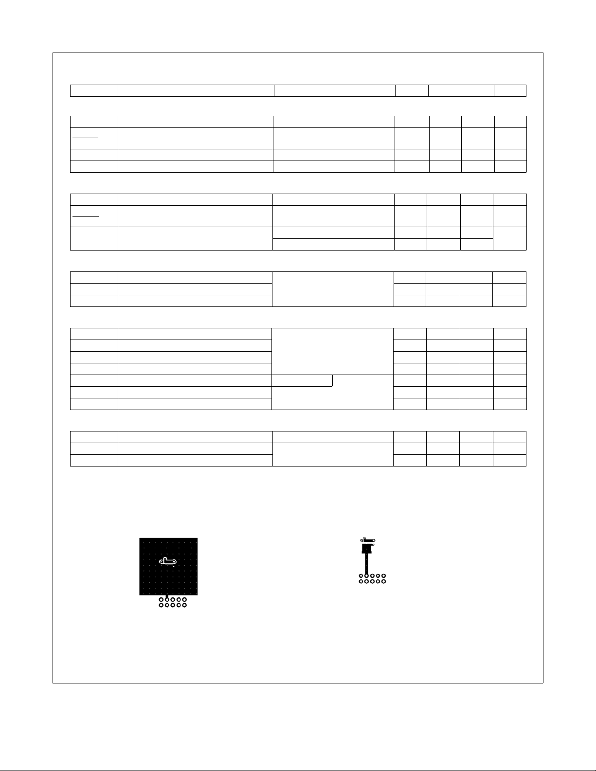
is determined with the device mounted on a 1 in2 oz copper pad on a 1.5 x 1.5 in. board of FR-4 material. R
= 60°C/W when mounted on a 1 in2 pad of 2 oz copper, 1.5’x1.5’x0.062’ thick PCB.
= 135°C/W when mounted on a minimum pad of 2 oz copper.
= 0V, IS = 2.2A (Note 2) 0.8 1.5 V
GS
IF = 1.0A, di/dt = 100A/μs
a. 60°C/W when mounted on
2
pad of 2 oz copper
a 1 in
60 ns
is guaranteed by design while R
θJC
b. 135°C/W when mounted on a
minimum pad of 2 oz copper
2
is determined by the
θJA
www.fairchildsemi.com

FDMC2674 N-Channel UltraFET Trench MOSFET
Typical Characteristics T
3.0
2.5
2.0
1.5
1.0
, DRAIN CURRENT (A)
D
I
0.5
0.0
0.0 0.5 1.0 1.5
VDS, DRAIN TO SOURCE VOLTAGE (V)
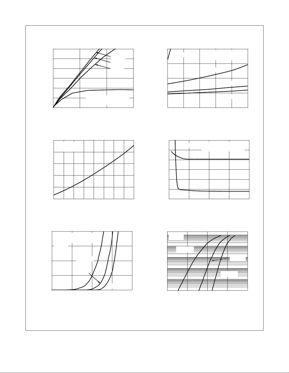
Figure 1.
On-Region Characteristics Figure 2.
2.4
ID = 1A
= 10V
V
2.0
GS
1.6
1.2
NORMALIZED
0.8
0.4
DRAIN TO SOURCE ON-RESISTANCE
-50 -25 0 25 50 75 100 125 150
TJ, JUNCTION TEMPERATURE (oC)
Fi g u re 3. N o rmal i z e d On - R e sist a n ce
vs Junction Temperature
PULSE DURATION = 80μs
DUTY CYCLE = 0.5%MAX
= 25°C unless otherwise noted
J
V
= 10V
GS
V
= 7V
GS
V
= 5V
GS
V
= 4.5V
GS
1.6
V
= 4.5V
GS
PULSE DURATION = 80μs
DUTY CYCLE = 0.5%MAX
1.4
VGS = 5.0V
1.2
NORMALIZED
1.0
0.8
DRAIN TO SOURCE ON-RESISTANCE
0.5 1.0 1.5 2.0 2.5 3.0
ID, DRAIN CURRENT(A)
V
VGS = 10V
Nor m a l i z e d On-Res i s t a n c e
vs Drain Current and Gate Voltage
0.8
0.7
(Ω)
ID = 1A
0.6
0.5
, DRAIN TO
0.4
DS(on)
R
0.3
SOURCE ON-RESISTANCE
0.2
4 8 12 16 20
VGS, GATE TO SOURCE VOLTAGE (V)
Figure 4.
On- Resistance vs Gate to
PULSE DURATION = 80μs
DUTY CYCLE = 0.5%MAX
TJ = 150oC
TJ = 25oC
Source Voltage
GS
= 7V
4
3
2
1
, DRAIN CURRENT (A)
D
I
0
FDMC2674 Rev.F
PULSE DURATION = 80μs
DUTY CYCLE = 0.5%MAX
V
= 5V
DD
TJ = 150oC
TJ = 25oC
TJ = -55oC
23456
VGS, GATE TO SOURCE VOLTAGE (V)
Figure 5. Transfer Characteristics
3
20
10
V
= 0V
GS
1
TJ = 150oC
0.1
0.01
TJ = -55oC
1E-3
, REVERSE DRAIN CURRENT (A)
S
I
1E-4
0.0 0.3 0.6 0.9 1.2
VSD, BODY DIODE FORWARD VOLTAGE (V)
Figure 6.
Source to Drain Diode
Forward Voltage vs Source Current
TJ = 25oC
www.fairchildsemi.com
 Loading...