Fairchild FDMC15N06 service manual

FDMC15N06
N-Channel MOSFET
55V, 15A, 0.090Ω
FDMC15N06 N-Channel MOSFET
July 2009
Features
•R
• 100% Avalanche Tested
• RoHS Compliant
= 0.075Ω ( Typ.)@ VGS = 10V, ID = 15A
DS(on)
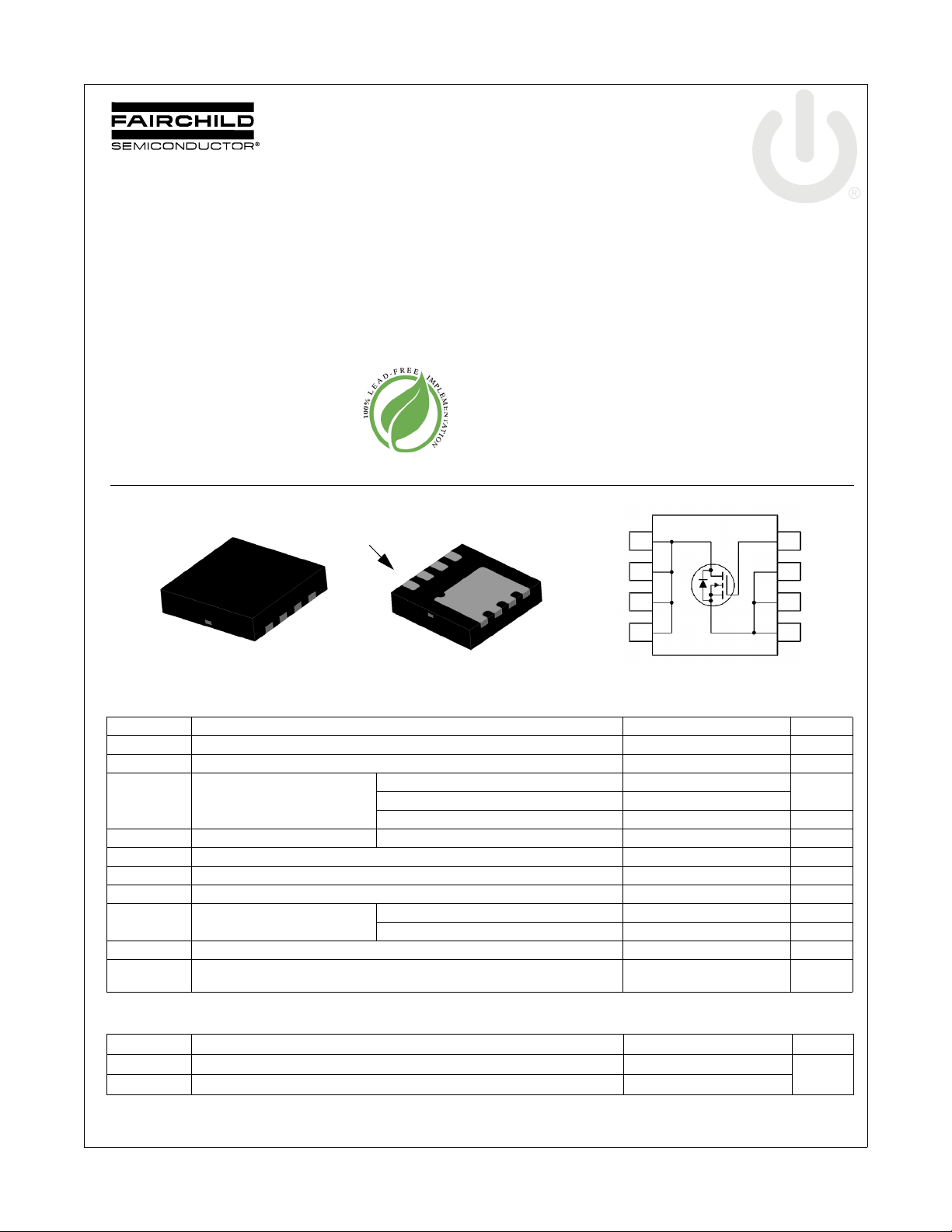
Top
Pin 1
Bottom
G
S
S
S
Description
These N-Channel power MOSFETs are manufactured using the
innovative UItraFET process. This advanced process technology
achieves the lowest possible on-resistance per silicon area,
resulting in outstanding performance.This device is capable of
withstanding high energy in the avalanche mode and the diode
exhibits very low reverse recovery time and stored charge. It was
designed for use in applications where power efficiency is
important, such as switching regulators, switching converters,
motor drivers, relay drivers, lowvoltage bus switches, and power
management in portable and battery-operated products.
5
D
D
6
D
D
D
D
D
7
8
D
4
3
2
1
MLP 3.3x3.3
MOSFET Maximum Ratings T
Symbol Parameter Ratings Units
V
V
I
I
E
I
E
P
T
T
DSS
GSS
D
DM
AS
AR
AR
D
J
L
, T
STG
Drain to Source Voltage 55 V
Gate to Source Voltage ±20 V
Drain Current
Drain Current - Pulsed (Note 2) 60 A
Single Pulsed Avalanche Energy (Note 3) 36 mJ
Avalanche Current 15 A
Repetitive Avalanche Energy 3.5 mJ
Power Dissipation
Operating and Storage Temperature Range -55 to +150
Maximum Lead Temperature for Soldering Purpose,
1/8” from Case for 5 Seconds
= 25oC unless otherwise noted
C
-Continuous (T
-Continuous (T
- Continuous (T
(T
= 25oC) 35 W
C
= 25oC) 2.3 W
(T
A
= 25oC) 15
C
= 100oC) 9
C
= 25oC) (Note 1a) 2.4 A
A
300
G
S
S
S
A
o
C
o
C
Thermal Characteristics
Symbol Parameter Ratings Units
R
θJC
R
θJA
©2009 Fairchild Semiconductor Corporation
FDMC15N06 Rev. A
Thermal Resistance, Junction to Case 3.5
Thermal Resistance, Junction to Ambient (Note 1a) 53
o
C/W
www.fairchildsemi.com1

Package Marking and Ordering Information
Device Marking Device Package Reel Size Tape Width Quantity
FDMC15N06 FDMC15N06 Power 33 13" 12mm 3000 units
FDMC15N06 N-Channel MOSFET
Electrical Characteristics T
= 25oC unless otherwise noted
C
Symbol Parameter Test Conditions Min. Typ. Max. Units
Off Characteristics
BV
∆BV
∆T
I
DSS
I
GSS
DSS
DSS
J
Drain to Source Breakdown Voltage ID = 250µA, VGS = 0V, TC = 25oC55 - - V
Breakdown Voltage Temperature
Coefficient
Zero Gate Voltage Drain Current
Gate to Body Leakage Current VGS = ±20V, V
I
= 250µA, Referenced to 25oC-70-V/
D
V
= 50V, V
DS
= 45V, TC = 150oC - - 250
V
DS
= 0V - - 1
GS
= 0V - - ±100 nA
DS
On Characteristics
V
GS(th)
R
DS(on)
g
FS
Gate Threshold Voltage VGS = VDS, ID = 250µA2.0-4.0V
Static Drain to Source On Resistance VGS = 10V, ID = 15A - 0.75 0.90 Ω
Forward Transconductance VDS = 20V, ID = 15A - 5 -S
Dynamic Characteristics
C
C
C
Q
Q
Q
iss
oss
rss
g(tot)
gs
gd
Input Capacitance
Output Capacitance - 97 130 pF
Reverse Transfer Capacitance - 28 42 pF
= 25V, VGS = 0V
V
DS
f = 1MHz
Total Gate Charge at 10V
V
= 30V,ID = 15A
Gate to Source Gate Charge - 1.7 - nC
Gate to Drain “Miller” Charge - 3.6 - nC
DS
V
= 10V
GS
(Note 4)
- 265 350 pF
- 8.8 11.5 nC
Switching Characteristics
t
d(on)
t
r
t
d(off)
t
f
Turn-On Delay Time
Turn-On Rise Time - 36.5 83 ns
Turn-Off Delay Time - 22.5 55 ns
Turn-Off Fall Time - 22 54 ns
= 30V, ID = 15A
V
DD
= 25Ω
R
G
(Note 4)
-9.529ns
µA
o
C
Drain-Source Diode Characteristics
I
S
I
SM
V
SD
t
rr
Q
rr
Notes:
1: R
is determined with the device mounted on a 1 in2 pad 2 oz copper pad on a 1.5 x 1.5 in. board of FR-4 material. R
θJA
the user's board design.
2: Repetitive Rating: Pulse width limited by maximum junction temperature
3: L = 1mH, I
4: Essentially Independent of Operating Temperature Typical Characteristics
5: ISD ≤ 15A, di/dt ≤ 200A/µs, VDD ≤ 40V, Starting TJ = 25°C
FDMC15N06 Rev. A
Maximum Continuous Drain to Source Diode Forward Current - - 15 A
Maximum Pulsed Drain to Source Diode Forward Current - - 60 A
Drain to Source Diode Forward Voltage V
Reverse Recovery Time
Reverse Recovery Charge - 35 - nC
a. 53 °C/W when mounted on
2
a 1 in
pad of 2 oz co pper
= 8.5A, RG = 25Ω, Starting TJ = 25°C
AS
= 0V, I
GS
V
= 0V, I
GS
dI
/dt = 100A/µs (Note 5)
F
= 15A - - 1.25 V
SD
= 15A
SD
2
-30-ns
is guaranteed by design while R
θJC
b.125 °C/W when mounted on
a minimum pad of 2 oz copper
is determined by
θCA
www.fairchildsemi.com

Typical Performance Characteristics
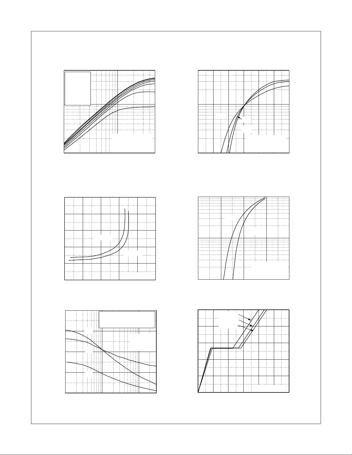
Figure 1. On-Region Characteristics Figure 2. Transfer Characteristics
50
V
15 V
10 V
8 V
7 V
6 V
5 V
10
GS
= 20 V
50
10
FDMC15N06 N-Channel MOSFET
, Drain Current[A]
D
I
*Notes:
1. 250
µs Pulse Test
= 25oC
2. T
1
0.1 1 5
C
VDS, Drain-Source Voltage[V]
, Drain Current[A]
D
I
1
2345678
150oC
25oC
-55oC
*Notes:
1. V
2. 250
= 20V
DS
µs Pulse Test
VGS, Gate-Source Voltage[V]
Figure 3. On-Resistance Variation vs. Figure 4. Body Diode Forward Voltage
Drain Current and Gate Voltage Variation vs. Source Current
and Temperature
0.25
0.20
0.15
[Ω],
0.10
DS(ON)
R
0.05
Drain-Source On-Resistance
0.00
0 1020304050
ID, Drain Current [A]
VGS = 10V
*Note: TC = 25oC
VGS = 20V
100
150oC
25oC
10
, Reverse Drain Current [A]
S
I
1
0.0 0.5 1.0 1.5 2.0
*Notes:
1. VGS = 0V
2. 250
µs Pulse Test
VSD, Body Diode Forward Voltage [V]
Figure 5. Capacitance Characteristics Figure 6. Gate Charge Characteristics
800
600
400
Capacitances [pF]
200
0
0.1 1 10
FDMC15N06 Rev. A
C
= Cgs + Cgd (Cds = shorted)
iss
C
= Cds + C
oss
C
C
C
rss
oss
C
iss
rss
= C
gd
gd
VDS, Drain-Source Voltage [V]
*Note:
1. V
= 0V
GS
2. f = 1MHz
10
VDS = 11V
V
= 30V
DS
= 44V
V
8
DS
6
4
, Gate-Source Voltage [V]
GS
V
2
0
024681012
*Note: ID = 15A
Qg, Total Gate Charge [nC]
3
www.fairchildsemi.com
 Loading...