Fairchild FDMB668P service manual

tm
FDMB668P
E
E
P-Channel 1.8V Logic Level PowerTrench® MOSFET
-20V, -6.1A, 35mΩ
Features
Max r
Max r
Max r
Excellent for portable application at V
Thin profile - Maximum height = 0.8mm
RoHS compliant
DS(on)
DS(on)
DS(on)
= 35mΩ at V
= 50mΩ at V
= 70mΩ at V
= -4.5V, ID = -6.1A
GS
= -2.5V, ID = -5.1A
GS
= -1.8V, ID = -4.3A
GS
GS
= -1.8V
General Description
FDMB668P is excellent for load switch and DC-DC conversion
among portable electronics. It achieves an optimal balance
among efficiency, thermal transfer and small form by integrating
a P-channel MOSFET with minimized on-state resistance into a
MicroFET 3x1.9 package. When optimizing the dimension of
portable applications, this little device offers a very efficient
solution.
Applications
Load Switch in:
-HDD
-Portable Gaming, MP3
-Notebook
DC/DC Conversion
FDMB668P P-Channel 1.8V Logic Level PowerTrench
February 2007
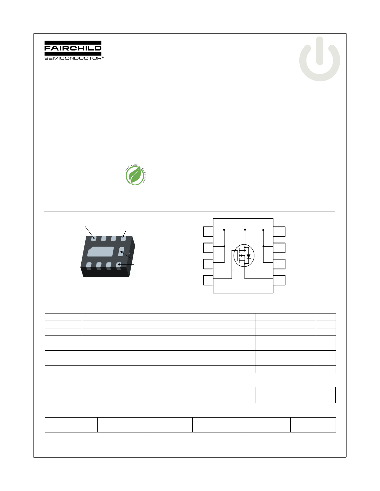
PIN 1
PIN 1
MicroFET 3X1.9
MOSFET Maximum Ratings T
Symbol Parameter Ratings Units
V
DS
V
GS
I
D
P
D
, T
T
J
STG
Drain to Source Voltage -20 V
Gate to Source Voltage ±8 V
Drain Current -Continuous (Note 1a) -6.1
-Pulsed -40
Power Dissipation (Note 1a) 1.9
Power Dissipation (Note 1b) 0.8
Operating and Storage Junction Temperature Range -55 to +150 °C
GATE
GATE
SOURC
SOURC
= 25°C unless otherwise noted
A
1
1
D
D
D
D
2
2
D
D
3
3
G
G
4
4
8
8
D
D
D
D
7
7
D
D
6
6
S
S
5
5
Thermal Characteristics
R
θJA
R
θJA
Thermal Resistance, Junction to Ambient (Note 1a) 65
Thermal Resistance, Junction to Ambient (Note 1b) 165
Package Marking and Ordering Information
®
MOSFET
A
W
°C/W
Device Marking Device Package Reel Size Tape Width Quantity
668 FDMB668P MicroFET 3X1.9 7” 8mm 3000 units
©2007 Fairchild Semiconductor Corporation
FDMB668P Rev.B
1
www.fairchildsemi.com

FDMB668P P-Channel 1.8V Logic Level PowerTrench
Electrical Characteristics T
= 25°C unless otherwise noted
J
Symbol Parameter Test Conditions Min Typ Max Units
Off Characteristics
BV
DSS
∆BV
DSS
∆T
J
I
DSS
I
GSS
On Characteristics
V
GS(th)
∆V
GS(th)
∆T
J
r
DS(on)
g
FS
Drain to Source Breakdown Voltage ID = -250µA, VGS = 0V -20 V
Breakdown Voltage Temperature
Coefficient
Zero Gate Voltage Drain Current VDS = -16V, V
Gate to Source Leakage Current VGS = ±8V, V
ID = -250µA, referenced to 25°C -11.4 mV/°C
= 0V -1 µA
GS
= 0V ±100 nA
DS
(Note 2)
Gate to Source Threshold Voltage VGS = VDS, ID = -250µA -0.4 -0.6 -1.0 V
Gate to Source Threshold Voltage
Temperature Coefficient
Static Drain to Source On Resistance
Forward Transconductance VDS = -4.5V, ID = -6.1A 27 S
ID = -250µA, referenced to 25°C 2.8 mV/°C
VGS = -4.5V, ID = -6.1A 22 35
VGS = -2.5V, ID = -5.1A 27 50
VGS = -1.8V, ID = -4.3A 35 70
VGS = -4.5V, ID = -6.1A,TJ = 125°C 31 50
Dynamic Characteristics
C
iss
C
oss
C
rss
Input Capacitance
Output Capacitance 210 280 pF
Reverse Transfer Capacitance 175 265 pF
VDS = -10V, VGS = 0V,
f = 1MHz
1565 2085 pF
Switching Characteristics
t
d(on)
t
r
t
d(off)
t
f
Q
Q
Q
Q
g
g
gs
gd
Turn-On Delay Time
Rise Time 9 18 ns
Turn-Off Delay Time 176 282 ns
VDD = -10V, ID = -6.1A
VGS = -4.5V, R
GEN
= 6Ω
7 14 ns
Fall Time 84 135 ns
Total Gate Charge VGS = 0V to -10V
Total Gate Charge VGS = 0V to -5V 22 31 nC
Gate to Source Gate Charge 3 nC
VDD = -10V
ID = -6.1A
42 59 nC
Gate to Drain “Miller” Charge 5 nC
mΩ
®
MOSFET
Drain-Source Diode Characteristics
V
SD
t
rr
Q
rr
Notes:
1: R
θJA
R
θJC
2: Pulse Test: Pulse Width < 300 us, Duty Cycle < 2%.
FDMB668P Rev.B
Source to Drain Diode Forward Voltage V
Reverse Recovery Time
Reverse Recovery Charge 15 23 nC
is the sum of the junction-to-case and case-to- ambient thermal resistance where the case thermal reference is defined as the solder mounting surface of the drain pins.
is guaranteed by design while R
is determined by the user’s board design.
θJA
GS
IF = -6.1A, di/dt = 100A/µs
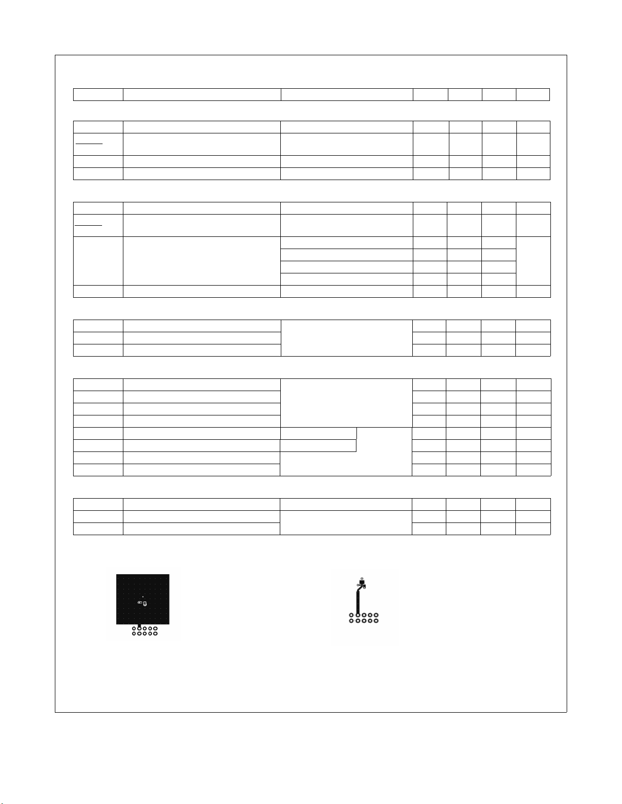
a) 65°C/W when mounted on a
2
pad of 2 oz copper
1in
= 0V, IS = -1.6A (Note 2) -0.7 -1.2 V
29 44 ns
b) 165°C/W when mounted on a
minimum pad .
2
www.fairchildsemi.com
 Loading...