Fairchild FDMA8884 service manual

FDMA8884
D
D
S
G
D
D
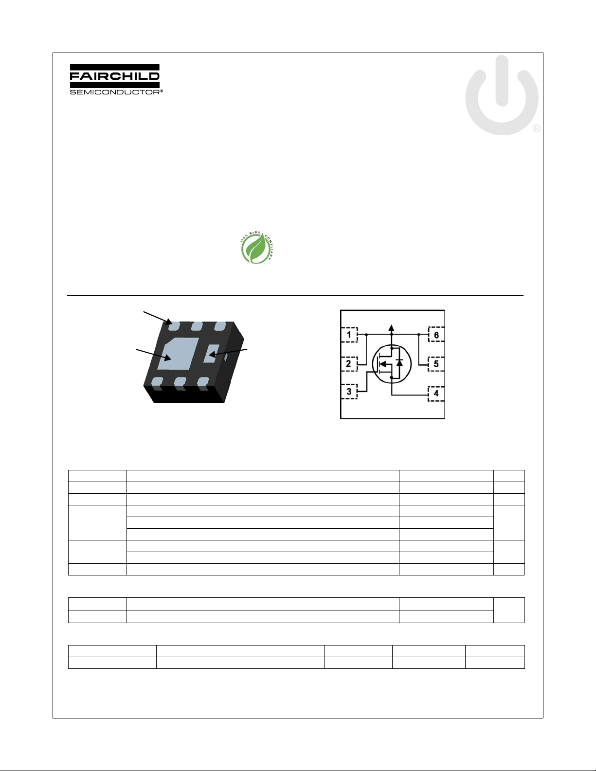
Pin 1
Drain
Source
MicroFET 2X2 (Bottom View)
Bottom Drain Contact
D
D
D
D
S
G
Single N-Channel Power Trench® MOSFET
30 V, 6.5 A, 23 mΩ
Features
Max r
Max r
High performance trench technology for extremely low r
Fast switching speed
RoHS Compliant
= 23 mΩ at VGS = 10 V, ID = 6.5 A
DS(on)
= 30 mΩ at VGS = 4.5 V, ID = 6.0 A
DS(on)
DS(on)
General Description
This N-Channel MOSFET is produced using Fairchild
Semiconductor‘s advanced Power Trench
been optimized for
Application
Primary Switch
r
switching performance.
DS(on)
April 2012
®
process that has
FDMA8884 N-Channel Power Trench
®
MOSFET
MOSFET Maximum Ratings T
Symbol Parameter Ratings Units
V
DS
V
GS
I
D
P
D
, T
T
J
STG
Drain to Source Voltage 30 V
Gate to Source Voltage (Note 3) ±20 V
Drain Current -Continuous (Package limited) TC = 25 °C 8.0
-Pulsed 25
Power Dissipation (Note 1a) 1.9
Power Dissipation (Note 1b) 0.7
Operating and Storage Junction Temperature Range -55 to +150 °C
= 25 °C unless otherwise noted
A
= 25 °C (Note 1a)
A
Thermal Characteristics
R
θJA
R
θJA
Package Marking and Ordering Information
Device Marking Device Package Reel Size Tape Width Quantity
©2012 Fairchild Semiconductor Corporation 1 www.fairchildsemi.com
FDMA8884 Rev.C3
Thermal Resistance, Junction to Ambient (Note 1a) 65
Thermal Resistance, Junction to Ambient (Note 1b) 180
884 FDMA8884 MicroFET 2x2 7 ’’ 12 mm 3000 units
°C/W
A6.5 -Continuous T
W

FDMA8884 N-Channel Power Trench
Electrical Characteristics T
= 25 °C unless otherwise noted
J
Symbol Parameter Test Conditions Min Typ Max Units
Off Characteristics
BV
ΔBV
ΔT
I
DSS
I
GSS
DSS
DSS
J
Drain to Source Breakdown Voltage ID = 250 μA, VGS = 0 V 30 V
Breakdown Voltage Temperature
Coefficient
Zero Gate Voltage Drain Current VDS = 24 V, V
Gate to Source Leakage Current, Forward VGS = 20 V, V
I
= 250 μA, referenced to 25 °C 15 mV/°C
D
= 0 V 1 μA
GS
= 0 V 100 nA
DS
On Characteristics
V
GS(th)
ΔV
ΔT
r
DS(on)
g
FS
GS(th)
J
Gate to Source Threshold Voltage VGS = VDS, ID = 250 μA1.21.83.0V
Gate to Source Threshold Voltage
Temperature Coefficient
Static Drain to Source On Resistance
I
= 250 μA, referenced to 25 °C -5 mV/°C
D
V
= 10 V, ID = 6.5 A 19 23
GS
= 4.5 V, ID = 6.0 A 25 30
GS
= 10 V, ID = 6.5 A, TJ = 125 °C 25 30
V
GS
Forward Transconductance VDD = 5 V, ID = 6.5 A 26 S
Dynamic Characteristics
C
iss
C
oss
C
rss
R
g
Input Capacitance
Output Capacitance 132 175 pF
Reverse Transfer Capacitance 18 28 pF
= 15 V, VGS = 0 V,
V
DS
f = 1 MHz
Gate Resistance 1.1 Ω
339 450 pF
Switching Characteristics
t
d(on)
t
r
t
d(off)
t
f
Q
Q
Q
g(TOT)
gs
gd
Turn-On Delay Time
Rise Time 110ns
Turn-Off Delay Time 11 20 ns
= 15 V, ID = 6.5 A,
V
DD
V
= 10 V, R
GS
GEN
= 6 Ω
510ns
Fall Time 110ns
Total Gate Charge VGS = 0 V to 10 V
Total Gate Charge V
Total Gate Charge 1.0 nC
= 0 V to 4.5 V 2.7 3.7 nC
GS
V
DD
I
= 6.5 A
D
= 15 V
5.4 7.5 nC
Gate to Drain “Miller” Charge 0.9 nC
mΩV
®
MOSFET
Drain-Source Diode Characteristics
V
SD
t
rr
Q
rr
NOTES:
is the sum of the junction-to-case and case-to-ambient thermal resistance where the case thermal reference is defined as the solder mounting surface of the drain pins.
1. R
θJA
R
is guaranteed by design while R
θJC
2. Pulse Test: Pulse Width < 300 μs, Duty cycle < 2.0 %.
3. As an N-ch device, the negative Vgs rating is for low duty cycle pulse occurrence only. No continuous rating is implied.
©2012 Fairchild Semiconductor Corporation 2 www.fairchildsemi.com
FDMA8884 Rev.C3
Source to Drain Diode Forward Voltage V
Reverse Recovery Time
Reverse Recovery Charge 4 10 nC
is determined by the user's board design.
θCA
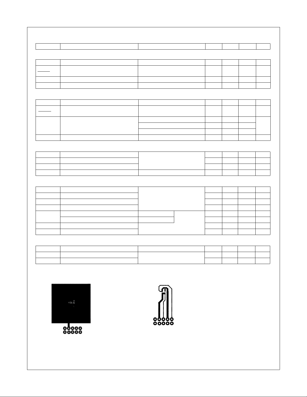
a. 65 °C/W when mounted
on a 1 in2 pad of 2 oz copper.
= 0 V, IS = 6.5 A (Note 2) 0.86 1.2 V
GS
= 6.5 A, di/dt = 100 A/μs
I
F
b. 180 °C/W when mounted on a
minimum pad of 2 oz copper.
16 28 ns
 Loading...