Fairchild FDMA520PZ service manual

April 2009
FDMA520PZ Single P-Channel PowerTrench
FDMA520PZ
Single P-Channel PowerTrench® MOSFET
–20V, –7.3A, 30m:
Features
Max r
Max r
Low profile - 0.8mm maximum - in the new package MicroFET
2X2 mm
HBM ESD protection level > 3k V typical (Note 3)
Free from halogenated compounds and antimony oxides
RoHS Compliant
= 30m: at VGS = –4.5V, ID = –7.3A
DS(on)
= 53m: at VGS = –2.5V, ID = –5.5A
DS(on)
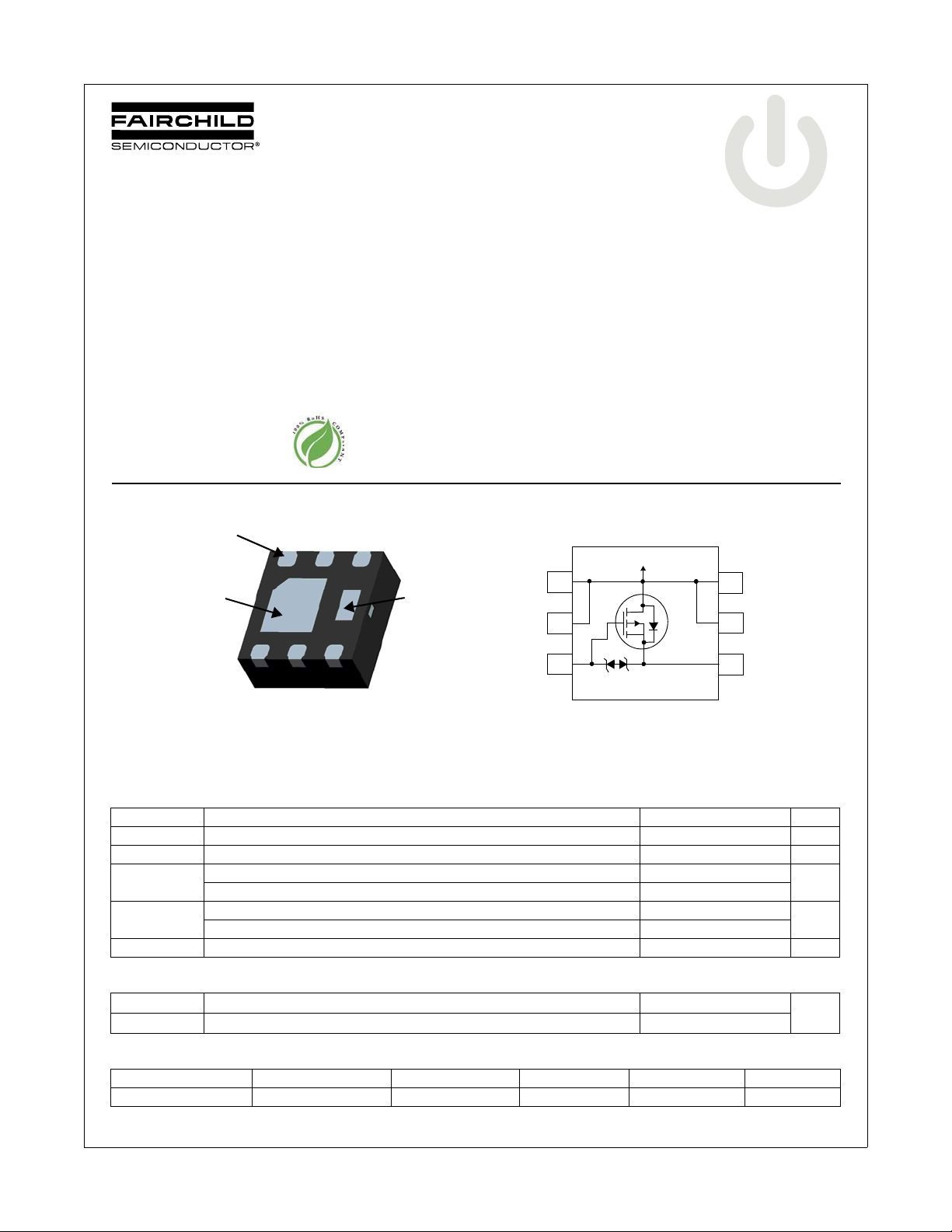
Pin 1
D
Drain
G
D
Source
General Description
This device is designed specifically for battery charge or load
switching in cellular handset and other ultraportable applications.
It features a MOSFET with low on-state resistance.
The MicroFET 2X2 package offers exceptional thermal
rmance for its physical size and is well suited to linear mo
perfo
applications.
D
D
Bottom Drain Contact
1
2
tm
de
®
MOSFET
6
D
5
D
3
G
D
S
D
4
S
MicroFET 2X2 (Bottom View)
MOSFET Maximum Ratings T
Symbol Parameter Ratings Units
V
DS
V
GS
I
D
P
D
, T
T
J
STG
Drain to Source Voltage –20 V
Gate to Source Voltage ±12 V
Drain Current -Continuous (Note 1a) –7.3
-Pulsed –24
Power Dissipation (Note 1a) 2.4
Power Dissipation (Note 1b) 0.9
Operating and Storage Junction Temperature Range –55 to +150 °C
= 25°C unless otherwise noted
A
Thermal Characteristics
R
TJA
R
TJA
Thermal Resistance, Junction to Ambient (Note 1a) 52
Thermal Resistance, Junction to Ambient (Note 1b) 145
Package Marking and Ordering Information
Device Marking Device Package Reel Size Tape Width Quantity
520 FDMA520PZ MicroFET 2X2 7’’ 8mm 3000 units
A
W
°C/W
©2009 Fairchild Semiconductor Corporation
FDMA520PZ Rev.B2
1
www.fairchildsemi.com

FDMA520PZ Single P-Channel PowerTrench
Electrical Characteristics T
= 25°C unless otherwise noted
J
Symbol Parameter Test Conditions Min Typ Max Units
Off Characteristics
BV
'BV
'T
I
DSS
I
GSS
DSS
DSS
J
Drain to Source Breakdown Voltage ID = –250PA, VGS = 0V –20 V
Breakdown Voltage Temperature
Coefficient
I
= –250PA, referenced to 25°C –8.4 mV/°C
D
Zero Gate Voltage Drain Current VDS = –16V, VGS = 0V –1 PA
Gate to Source Leakage Current VGS = ±12V, V
= 0V ±10 PA
DS
On Characteristics
V
GS(th)
'V
'T
r
DS(on)
g
FS
GS(th)
J
Gate to Source Threshold Voltage VGS = VDS, ID = –250PA –0.6 –1.1 –1.5 V
Gate to Source Threshold Voltage
Temperature Coefficient
Static Drain to Source On Resistance
= –250PA, referenced to 25°C 3.5 mV/°C
I
D
V
= –4.5V, ID = –7.3A 26 30
GS
= –2.5V, ID = –5.5A 42 53
GS
= –4.5V, ID = –7.3A ,TJ = 125°C 36 55
V
GS
Forward Transconductance VDS = –5V, ID = –7.3A 22 S
Dynamic Characteristics
C
iss
C
oss
C
rss
Input Capacitance
Output Capacitance 255 340 pF
Reverse Transfer Capacitance 225 340 pF
V
= –10V, VGS = 0V,
DS
f = 1MHz
1235 1645 pF
Switching Characteristics
t
d(on)
t
r
t
d(off)
t
f
Q
Q
Q
Turn-On Delay Time
Rise Time 29 47 ns
Turn-Off Delay Time 83 133 ns
VDD = –10V, ID = –7.3A
= –4.5V, R
V
GS
GEN
= 6:
Fall Time 74 119 ns
g
gs
gd
Total Gate Charge
Gate to Source Gate Charge 2.9 nC
Gate to Drain “Miller” Charge 4.4 nC
V
= –5V, ID = –7.3A
DD
= –4.5V
V
GS
10 20 ns
14 20 nC
m:V
®
MOSFET
Drain-Source Diode Characteristics
I
S
V
SD
t
rr
Q
rr
Notes:
1: R
is the sum of the junction-to-case and case-to-ambient thermal resistance where the case thermal reference is defined as the solder mounting surface of the drain pins.
TJA
2: Pulse Test: Pulse Width < 300Ps, Duty cycle < 2.0%.
3: The diode connected between the gate and the source serves only as protection against ESD. No gate overvoltage rating is implied.
FDMA520PZ Rev.B2
Maximum Continuous Drain-Source Diode Forward Current –2 A
Source to Drain Diode Forward Voltage VGS= 0V, IS= –2A –0.8 –1.2 V
Reverse Recovery Time
Reverse Recovery Charge 22 33 nC
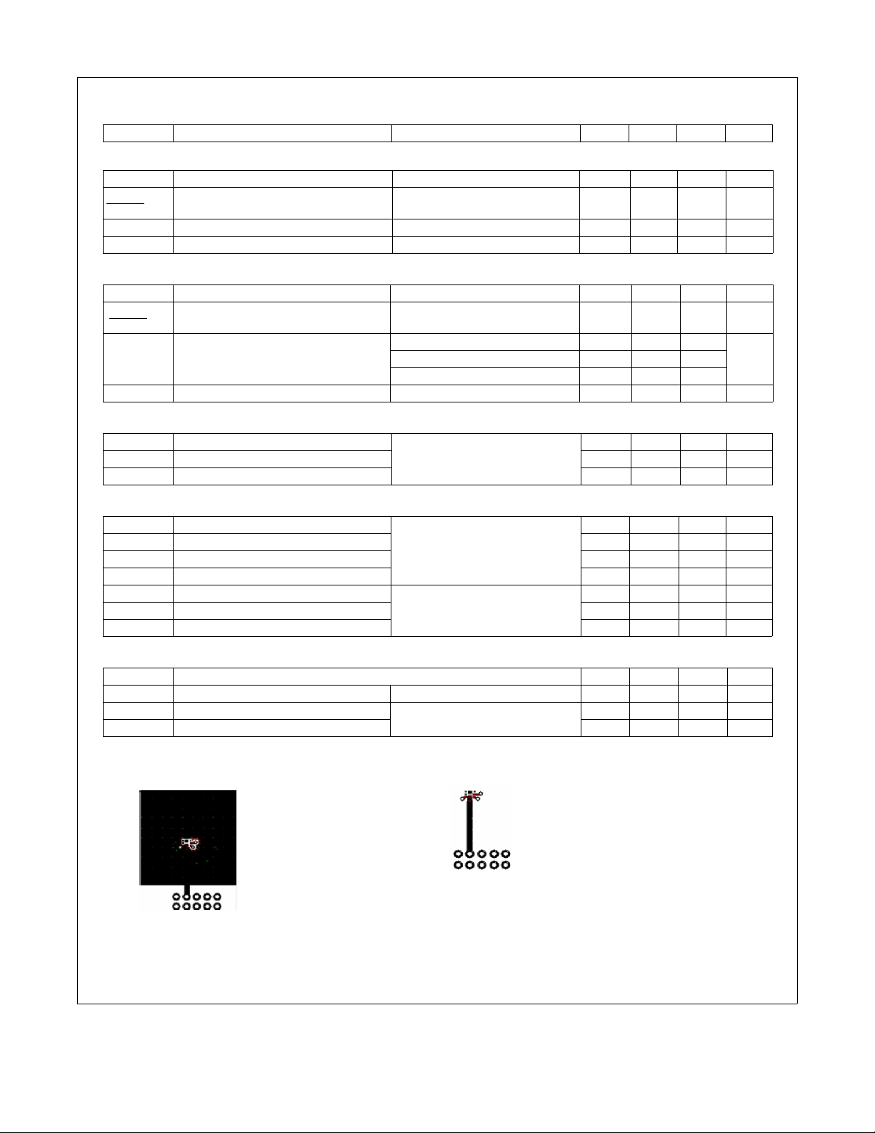
a. 52°C/W when mounted on
2
pad of 2 oz copper
a 1 in
=–7.3A, di/dt = 100A/Ps
I
F
2
b.145°C/W when mounted on a
minimum pad of 2 oz copper
30 45 ns
www.fairchildsemi.com
 Loading...