Fairchild FDMA3027PZ service manual

FDMA3027PZ
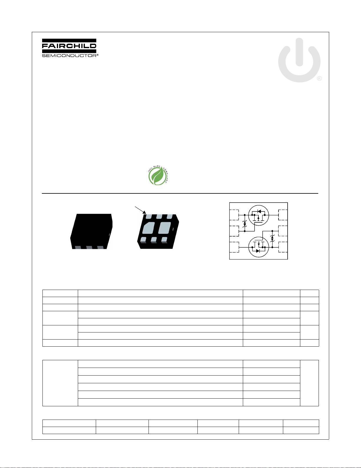
G2
S1
G1
D2
D1
S2
S1 G1 D2
S2
MicroFET 2x2
D1 G2
PIN 1
D1 D2
Top Bottom
1
2
3
6
5
4
Dual P-Channel PowerTrench® MOSFET
-30 V, -3.3 A, 87 mΩ
Features
Max r
Max r
HBM ESD protection level > 2 KV typical (Note 3)
Low profile - 0.8 mm maximum - in the new package
MicroFET 2x2 mm
RoHS Compliant
= 87 mΩ at VGS = -10 V, ID = -3.3 A
DS(on)
= 152 mΩ at VGS = -4.5 V, ID = -2.3 A
DS(on)
General Description
This device is designed specifically as a single package solution
for dual switching requirements such as gate driver for larger
Mosfets. It features two independent P-Channel MOSFETs with
low on-state resistance for minimum conduction losses. The
MicroFET 2x2 package offers exceptional thermal performance
for its physical size and is well suited to linear mode applications.
G-S zener has been added to enhance ESD voltage level.
Applications
Load Switch
Discrete Gate Driver
FDMA3027PZ Dual P-Channel PowerTrench
June 2012
®
MOSFET
MOSFET Maximum Ratings T
Symbol Parameter Ratings Units
V
DS
V
GS
I
D
P
D
, T
T
J
STG
Thermal Characteristics
R
θJA
Package Marking and Ordering Information
Device Marking Device Package Reel Size Tape Width Quantity
©2012 Fairchild Semiconductor Corporation
FDMA3027PZ Rev.C
Drain to Source Voltage -30 V
Gate to Source Voltage ±25 V
Drain Current -Continuous (Note 1a) -3.3
-Pulsed -15
Power Dissipation (Note 1a) 1.4
Power Dissipation (Note 1b) 0.7
Operating and Storage Junction Temperature Range -55 to +150 °C
Thermal Resistance for Single Operation, Junction to Ambient (Note 1a) 86
Thermal Resistance for Single Operation, Junction to Ambient (Note 1b) 173
Thermal Resistance for Dual Operation, Junction to Ambient (Note 1c) 69
Thermal Resistance for Dual Operation, Junction to Ambient (Note 1d) 151
Thermal Resistance for Single Operation, Junction to Ambient (Note 1e) 160
Thermal Resistance for Dual Operation, Junction to Ambient (Note 1f) 133
327 FDMA3027PZ MicroFET 2X2 7 ’’ 8 mm 3000 units
= 25 °C unless otherwise noted
A
1
A
W
°C/W
www.fairchildsemi.com

FDMA3027PZ Dual P-Channel PowerTrench
Electrical Characteristics T
= 25 °C unless otherwise noted
J
Symbol Parameter Test Conditions Min Typ Max Units
Off Characteristics
BV
ΔBV
ΔT
I
DSS
I
GSS
DSS
DSS
J
Drain to Source Breakdown Voltage ID = -250 μA, VGS = 0 V -30 V
Breakdown Voltage Temperature
Coefficient
Zero Gate Voltage Drain Current VDS = -24 V, V
Gate to Source Leakage Current VGS = ±25 V, V
I
= -250 μA, referenced to 25 °C -22 mV/°C
D
= 0 V -1 μA
GS
= 0 V ±10 μA
DS
On Characteristics
V
GS(th)
ΔV
ΔT
r
DS(on)
g
FS
GS(th)
J
Gate to Source Threshold Voltage VGS = VDS, ID = -250 μA-1-1.9-3V
Gate to Source Threshold Voltage
Temperature Coefficient
Static Drain to Source On Resistance
I
= -250 μA, referenced to 25 °C 5 mV/°C
D
V
= -10 V, ID = -3.3 A 69 87
GS
= -4.5 V, ID = -2.3 A 108 152
GS
= -10 V, ID = -3.3 A, TJ = 125 °C 97 122
V
GS
Forward Transconductance VDS = -5 V, ID = -3.3 A 6 S
Dynamic Characteristics
C
iss
C
oss
C
rss
R
g
Input Capacitance
Output Capacitance 59 80 pF
Reverse Transfer Capacitance 53 80 pF
= -15 V, VGS = 0 V,
V
DS
f = 1 MHz
Gate Resistance 12 Ω
324 435 pF
Switching Characteristics
t
d(on)
t
r
t
d(off)
t
f
Q
g(TOT)
Q
gs
Q
gd
Turn-On Delay Time
Rise Time 310ns
Turn-Off Delay Time 17 31 ns
= -15 V, ID = -3.3 A,
V
DD
V
= -10 V, R
GS
GEN
= 6 Ω
Fall Time 11 25 ns
Total Gate Charge V
Total Gate Charge V
Gate to Source Charge 1.0 nC
= 0 V to -10 V
GS
= 0 V to -5 V 4.1 6 nC
GS
= -15 V,
V
DD
I
= -3.3 A
D
Gate to Drain “Miller” Charge 1.9 nC
5.2 11 ns
7.2 10 nC
mΩV
®
MOSFET
Drain-Source Diode Characteristics
V
SD
t
rr
Q
rr
©2012 Fairchild Semiconductor Corporation
FDMA3027PZ Rev.C
Source to Drain Diode Forward Voltage V
Reverse Recovery Time
Reverse Recovery Charge 10 18 nC
= 0 V, IS = -3.3 A (Note 2) -0.94 -1.3 V
GS
= -3.3 A, di/dt = 100 A/μs
I
F
2
20 32 ns
www.fairchildsemi.com

FDMA3027PZ Dual P-Channel PowerTrench
Electrical Characteristics T
Notes:
1. R
is determined with the device mounted on a 1 in2 oz. copper pad on a 1.5 x 1.5 in. board of FR-4 material. R
θJA
user's board design.
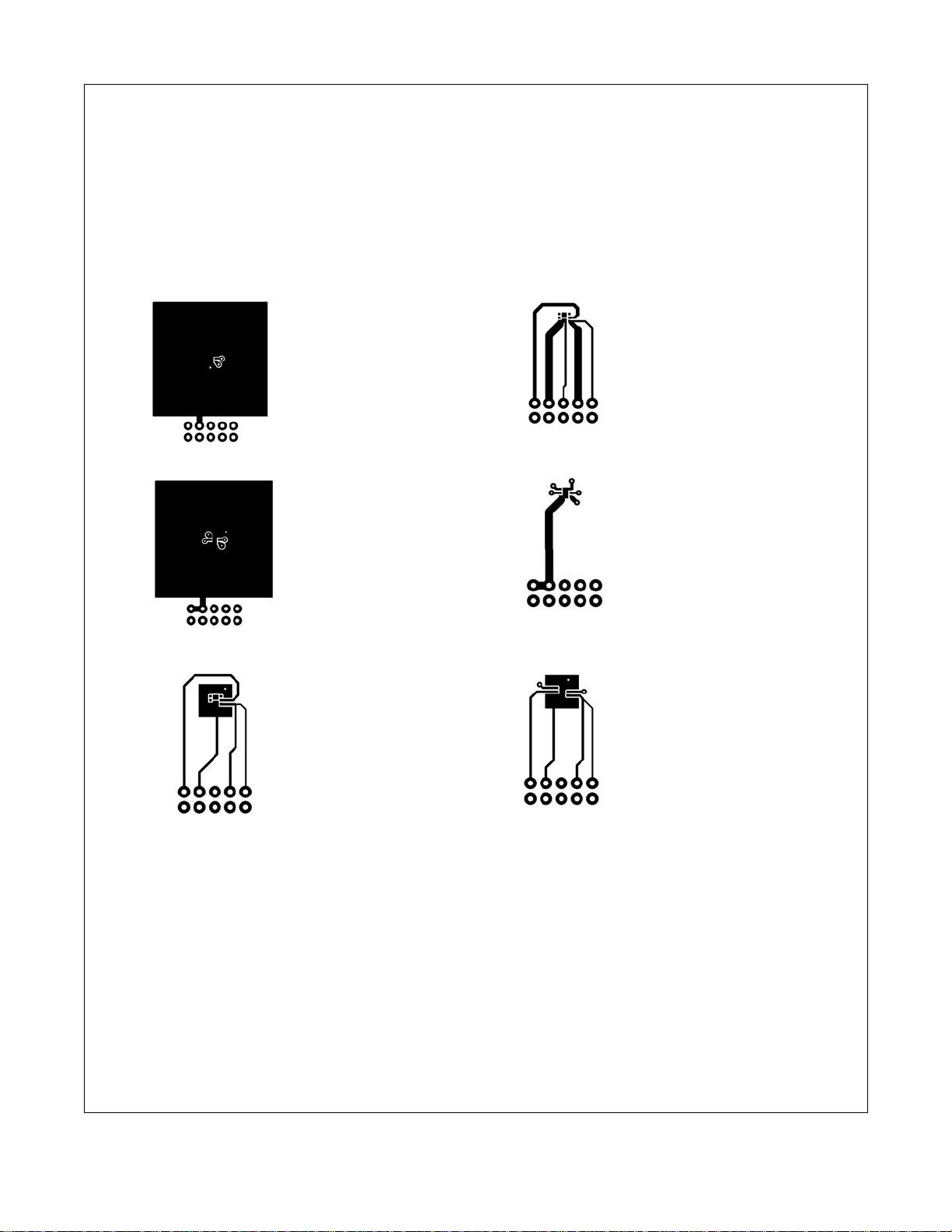
(a) R
(b) R
(c) R
(d) R
(e) R
(f) R
= 86 °C/W when mounted on a 1 in2 pad of 2 oz copper, 1.5 " x 1.5 " x 0.062 " thick PCB. For single operation.
θJA
= 173 °C/W when mounted on a minimum pad of 2 oz copper. For single operation.
θJA
= 69 oC/W when mounted on a 1 in
θJA
= 151 oC/W when mounted on a minimum pad of 2 oz copper. For dual operation.
θJA
= 160 oC/W when mounted on a 30 mm2 pad of 2 oz copper. For single operation.
θJA
= 133 oC/W when mounted on a 30 mm2 pad of 2 oz copper. For dual operation.
θJA
a. 86 °C/W when mounted on
a 1 in
c. 69 °C/W when mounted on
a 1 in
= 25 °C unless otherwise noted
J
2
pad of 2 oz copper, 1.5 ” x 1.5 ” x 0.062 ” thick PCB. For dual operation.
2
pad of 2 oz copper
2
pad of 2 oz copper
is guaranteed by design while R
θJC
b. 173 °C/W when mounted on
a minimum pad of 2 oz copper
d. 151 °C/W when mounted on
a minimum pad of 2 oz copper
is determined by the
θJA
®
MOSFET
e. 160 °C/W when mounted on
30 mm2 pad of 2 oz copper
2. Pulse Test : Pulse Width < 300 us, Duty Cycle < 2.0%
3. The diode connected between gate and source serves only as protection against ESD. No gate overvoltage rating is implied.
©2012 Fairchild Semiconductor Corporation
3
FDMA3027PZ Rev.C
f. 133 °C/W when mounted on
30 mm2 pad of 2 oz copper
www.fairchildsemi.com
 Loading...