Fairchild FDMA2002NZ service manual

FDMA2002NZ Dual N-Channel PowerTrench
FDMA2002NZ
Dual N-Channel PowerTrench MOSFET
General Description
This device is designed specifically as a single package
solution for dual switching requirements in cellular
handset and other ultra-portable applications. It
features two independent N-Channel MOSFETs with
low on-state resistance for minimum conduction losses.
The MicroFET 2x2 offers exceptional thermal
performance for its physical size and is well suited to
linear mode applications.
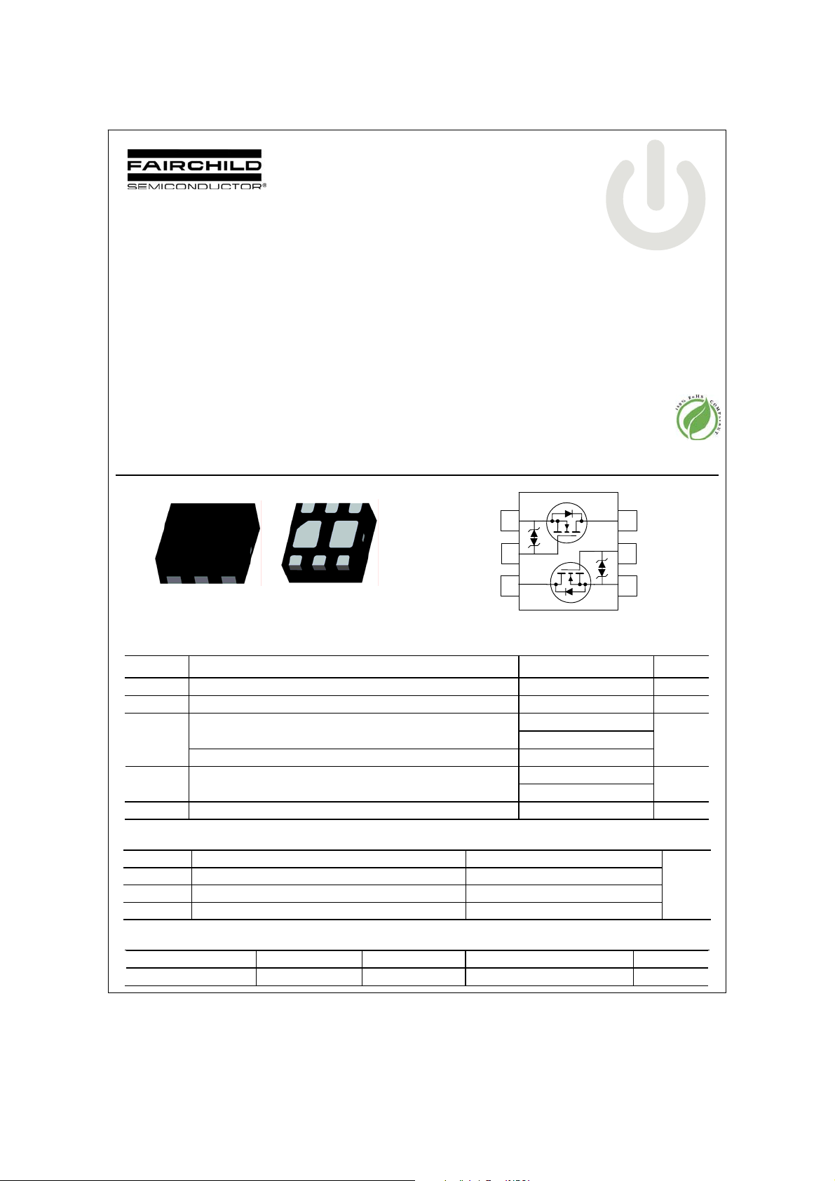
PIN 1
S1 G1 D2
D1 D2
MicroFET 2x2
D1 G2 S2
May 200
tm
t
tm
tm
Features
x 2.9 A, 30 V R
R
R
x Low profile – 0.8 mm maximum – in the new package
MicroFET 2x2 mm
x HBM ESD protection level = 1.8kV (Note 3)
x RoHS Compliant
Free from halogenated compounds and antimony
oxides
S1
G1
D2
= 123 m: @ VGS = 4.5 V
DS(ON)
= 140 m: @ VGS = 3.0 V
DS(ON)
= 163 m: @ VGS = 2.5 V
DS(ON)
1
2
3
D1
6
5
G2
4
S2
MOSFET
Absolute Maximum Ratings T
=25oC unless otherwise noted
A
Symbol Parameter Ratings Units
VDS Drain-Source Voltage 30 V
VGS Gate-Source Voltage
I
D
D
TJ, T
Drain Current – Continuous (TC = 25°C, VGS = 4.5V) 2.9
– Continuous (TC = 25°C, VGS = 2.5V) 2.7
– Pulsed 10
Power Dissipation for Single Operation (Note 1a) 1.5 P
Power Dissipation for Single Operation
Operating and Storage Temperature –55 to +150
STG
(Note 1b) 0.65
r12
Thermal Characteristics
R
TJA
R
TJA
R
TJA
R
TJA
Thermal Resistance, Junction-to-Ambient
Thermal Resistance, Junction-to-Ambient
Thermal Resistance, Junction-to-Ambient
Thermal Resistance, Junction-to-Ambient
(Note 1a) 83 (Single Operation)
(Note 1b) 193 (Single Operation)
(Note 1c) 68 (Dual Operation)
(Note 1d) 145 (Dual Operation)
Package Marking and Ordering Information
Device Marking Device Reel Size Tape width Quantity
002 FDMA2002NZ 7’’ 8mm 3000 units
20 Fairchild Semiconductor Corpora tion
FDMA2002NZ Rev B (W)
V
A
W
qC
qC/W

FDMA2002NZ Dual N-Channel PowerTrench
Electrical Characteristics T
= 25°C unless otherwise noted
A
Symbol Parameter Test Conditions Min Typ Max Units
Off Characteristics
BV
DSS
'BVDSS
'T
J
I
Zero Gate Voltage Drain Current VDS = 24 V, VGS = 0 V 1
DSS
I
Gate–Body Leakage Current VGS = ± 12 V, VDS = 0 V ±10
GSS
Drain–Source Breakdown Voltage
Breakdown Voltage Temperature
Coefficient
= 0 V, ID = 250 PA
V
GS
I
= 250 PA, Referenced to 25°C
D
30 V
25 mV/°C
PA
PA
On Characteristics
V
Gate Threshold Voltage
GS(th)
'VGS(th)
'T
J
R
DS(on)
Gate Threshold Voltage
Temperature Coefficient
Static Drain–Source
On–Resistance
= VGS, ID = 250 PA
V
DS
= 250 PA, Referenced to 25°C
I
D
VGS = 4.5V, ID = 2.9A 75 123
VGS = 3.0V, ID = 2.7A 84 140
VGS = 2.5V, ID = 2.5A 92 163
VGS = 4.5V, ID = 2.9A, TC = 85°C 95 166
VGS = 3.0V, ID = 2.7A, TC = 150°C 138 203
= 2.5V, ID = 2.5A, TC = 150°C 150 268
V
GS
0.4 1.0 1.5 V
–3
mV/qC
m:
Dynamic Characteristics
C
Input Capacitance 190 220 pF
iss
C
Output Capacitance 30 40 pF
oss
C
Reverse Transfer Capacitance
rss
V
= 15 V, V
DS
f = 1.0 MHz
GS
= 0 V,
20 30 pF
Switching Characteristics (Note 2)
= 15 V, ID = 1 A,
t
Turn–On Delay Time 6 12 ns
d(on)
t
r
t
Turn–Off Delay Time 12 21 ns
d(off)
Turn–On Rise Time 8 16 ns
tf Turn–Off Fall Time
Qg Total Gate Charge 2.4 3.0 nC
Qgs Gate–Source Charge 0.35 nC
Qgd Gate–Drain Charge
V
DD
= 4.5 V, R
V
GS
= 15 V, ID = 2.9 A,
V
DS
V
= 4.5 V
GS
GEN
= 6 :
2 10 ns
0.75 nC
Drain–Source Diode Characteristics and Maximum Ratings
IS Maximum Continuous Source–Drain Diode Forward Current 2.9 A
V
SD
trr Diode Reverse Recovery Time 10 ns
Qrr Diode Reverse Recovery Charge
Source–Drain Diode Forward
Voltage
IS = 2.0 A 0.9 1.2
I
= 1.1 A 0.8 1.2
S
= 2.9 A,
I
F
dI
/dt = 100 A/μs
F
2 nC
V
MOSFET
FDMA2002NZ Rev B (W)
 Loading...