FDMA1032CZ
FDMA1032CZ 20V Complementary PowerTrench
May 2010
20V Complementary PowerTrench MOSFET
General Description
This device is designed specifically as a single package
solution for a DC/DC 'Switching' MOSFET in cellular
handset and other ultra-portable applications. It
features an independent N-Channel & P-Channel
MOSFET with low on-state resistance for minimum
conduction losses. The gate charge of each MOSFET
is also minimized to allow high frequency switching
directly from the controlling device. The MicroFET 2x2
package offers exceptional thermal performance for its
physical size and is well suited to switching applications.
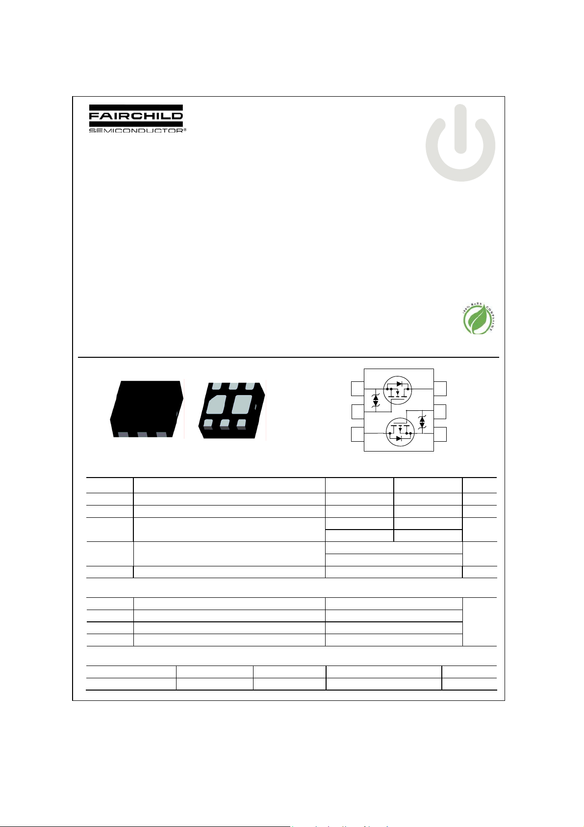
PIN 1
S1 G1 D2
D1 D2
D1 G2 S2
Features
x Q1: N-Channel
3.7 A, 20V. R
R
x Q2: P-Channel
–3.1 A, –20V. R
R
x Low profile – 0.8 mm maximum – in the new package
MicroFET 2x2 mm
HBM ESD protection level >2kV (Note 3)
x RoHS Compliant
Free from halogenated compounds and antimony
oxides
S1
G1
D2
= 68 m: @ VGS = 4.5V
DS(ON)
= 86 m: @ VGS = 2.5V
DS(ON)
= 95 m: @ VGS = –4.5V
DS(ON)
= 141 m: @ VGS = –2.5V
DS(ON)
1
2
3
6
D1
5
G2
4
S2
tm
MOSFET
MicroFET 2x2
Absolute Maximum Ratings T
=25oC unless otherwise noted
A
Symbol Parameter Q1 Q2 Units
VDS Drain-Source Voltage 20 –20 V
VGS Gate-Source Voltage
I
D
P
D
TJ, T
STG
Drain Current – Continuous (Note 1a) 3.7 –3.1
– Pulsed 6 –6
Power Dissipation for Single Operation (Note 1a) 1.4
(Note 1b)
Operating and Storage Junction Temperature Range –55 to +150
r12
0.7
±12 V
A
W
qC
Thermal Characteristics
R
TJA
R
TJA
R
TJA
R
TJA
Thermal Resistance, Junction-to-Ambient
Thermal Resistance, Junction-to-Ambient
Thermal Resistance, Junction-to-Ambient
Thermal Resistance, Junction-to-Ambient
(Note 1a) 86 (Single Operation)
(Note 1b) 173 (Single Operation)
(Note 1c) 69 (Dual Operation)
(Note 1d) 151 (Dual Operation)
Package Marking and Ordering Information
Device Marking Device Reel Size Tape width Quantity
032 FDMA1032CZ 7’’ 8mm 3000 units
2010 Fairchild Semiconductor Corpora tion
qC/W
FDMA1032CZ Rev B4 (W)

FDMA1032CZ 20V Complementary PowerTrench
Electrical Characteristics T
= 25°C unless otherwise noted
A
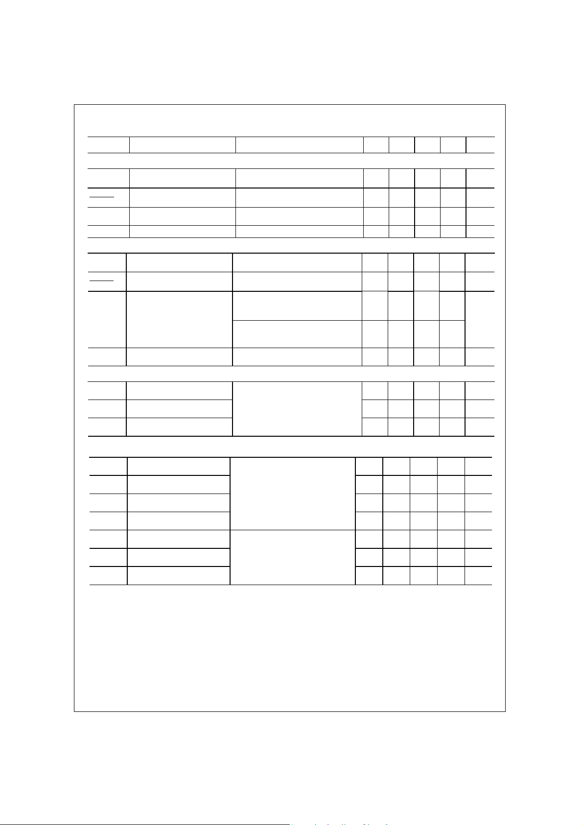
Symbol Parameter Test Conditions Type Min Typ Max Units
Off Characteristics
BV
DSS
'BVDSS
'T
I
Zero Gate Voltage Drain
DSS
I
Gate-Body Leakage VGS = ±12 V, VDS = 0 V All ±10
GSS
Drain-Source Breakdown
Voltage
Breakdown Voltage
Temperature Coefficient
J
Current
V
= 0 V, ID = 250 PA
GS
= 0 V, ID = –250 PA
V
GS
= 250 PA, Referenced to 25qC
I
D
I
= –250 μA, Referenced to 25qC
D
VDS = 16 V, VGS = 0 V
= –16 V, VGS = 0 V
V
DS
Q1Q220
–20
Q1
Q2
Q1
Q2
V
15
mV/qC
–12
1
–1
PA
PA
On Characteristics (Note 2)
V
Gate Threshold Voltage
GS(th)
'VGS(th)
'T
R
DS(on)
Gate Threshold Voltage
Temperature Coefficient
J
Static Drain-Source
On-Resistance
V
= VGS, ID = 250 PA
DS
V
= VGS, ID = –250 μA
DS
I
= 250 PA, Referenced to 25qC
D
= –250 μA, Referenced to 25qC
I
D
VGS = 4.5 V, ID = 3.7 A
= 2.5 V, ID = 3.3 A
V
GS
= 4.5 V, ID = 3.7 A, TJ = 125qC
V
GS
= –4.5V, ID = –3.1 A
V
GS
= –2.5 V, ID = –2.5 A
V
GS
= –4.5 V, ID = –3.1 A,TJ = 125qC
V
GS
gFS Forward Transconductance VDS = 10 V, ID = 3.7 A
V
= –10 V, ID = –3.1 A
DS
Q1Q20.6
Q1
Q2
Q1 37
Q2 60
Q1
Q2
1.0
–0.6
–1.0
–4
4
50
53
88
87
16
–11
1.5
V
–1.5
mV/qC
68
m:
86
90
95
m:
141
140
S
Dynamic Characteristics
C
Input Capacitance Q1
iss
C
Output Capacitance Q1
oss
C
Reverse Transfer
rss
Capacitance
Q1
V
= 10 V, VGS = 0 V, f = 1.0 MHz
DS
Q2
V
= –10 V, VGS = 0 V, f = 1.0 MHz
DS
Q2
Q2
Q1
Q2
340
540
80
120
60
100
pF
pF
pF
Switching Characteristics (Note 2)
Turn-On Delay Time Q1
t
d(on)
tr Turn-On Rise Time Q1
t
Turn-Off Delay Time Q1
d(off)
tf Turn-Off Fall Time
Qg Total Gate Charge Q1
Qgs Gate-Source Charge Q1
Qgd Gate-Drain Charge
Q1
V
= 10 V, ID = 1 A,
DD
= 4.5 V, R
V
GS
GEN
= 6 :
Q2
= –10 V, ID = –1 A,
V
DD
V
= –4.5 V, R
GS
GEN
= 6 :
Q1
V
= 10 V, ID = 3.7 A, VGS = 4.5 V
DS
Q2
V
= –10 V,ID =– 3.1 A,
DS
V
=– 4.5 V
GS
Q2
Q2
Q2
Q1
Q2
Q2
Q2
Q1
Q2
8 131624ns
8 111620ns
14 372659ns
3 366
ns
58
4 76
nC
10
0.7
nC
1.1
1.1
nC
2.4
MOSFET
FDMA1032CZ Rev B4 (W)

FDMA1032CZ 20V Complementary PowerTrench
Electrical Characteristics T
= 25°C unless otherwise noted
A
Symbol Parameter Test Conditions Type Min Typ Max Units
Drain–Source Diode Characteristics and Maximum Ratings
I
Maximum Continuous Source-Drain Diode Forward Current Q1
S
V
SD
trr Diode Reverse Recovery
Qrr Diode Reverse Recovery
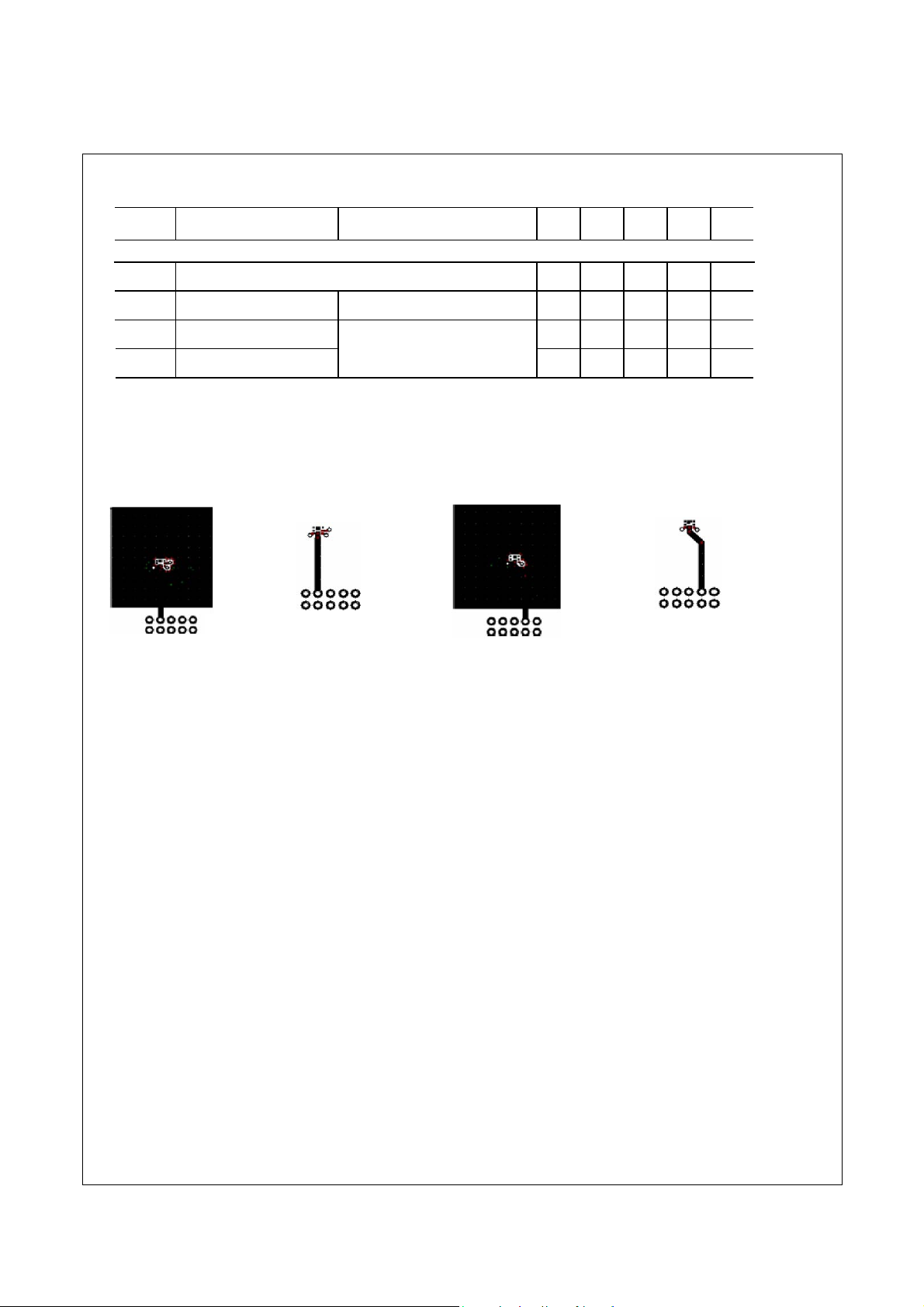
Notes:
1. R
TJA
user's board design.
(a) R
(b) R
(c) R
(d) R
2. Pulse Test : Pulse Width < 300 us, Duty Cycle < 2.0%
3. The diode connected between the gate and source serves only as protection against ESD. No gate overvoltage rating is implied.
Source-Drain Diode Forward
Voltage
VGS = 0 V, IS = 1.1 A (Note 2)
VGS = 0 V, IS = –1.1 A (Note 2)
Q1
Time
Charge
is determined with the device m ounted on a 1 in2 oz. copper pad on a 1.5 x 1.5 in. board of FR-4 material. R
= 86 °C/W when mounted on a 1 in2 pad of 2 oz copper, 1.5 " x 1.5 " x 0.062 " thick PCB. For single operation.
TJA
= 173 °C/W when mounted on a minimum pad of 2 oz copper. For single operation.
TJA
= 69 oC/W when mounted on a 1 in2pad of 2 oz copper, 1.5 ” x 1.5 ” x 0.062 ” thick PCB. For dual operation.
TJA
= 151 oC/W when mounted on a minimum pad of 2 oz copper. For dual operation.
TJA
a)86 oC/W when
mounted on a 1
2
in
pad of 2 oz
copper.
I
= 3.7 A, dIF/dt = 100 A/μs
F
Q2
I
= –3.1 A, dIF/dt = 100 A/μs
F
o
C/W when
b)173
mounted on a
minimum pad of 2
oz copper.
Q2
Q1
Q2
Q1
Q2
Q1
Q2
1.1
–1.1
0.7
–0.8
1.2
–1.2
11 25 ns
2 9 nC
is guaranteed by design while R
TJC
o
C/W when
c)69
mounted on a 1 in
pad of 2 oz copper.
2
TJA
A
V
is determined by the
o
C/W when
d)151
mounted on a
minimum pad of 2 oz
copper.
MOSFET
FDMA1032CZ Rev B4 (W)
 Loading...