Fairchild FDMA1023PZ service manual

FDMA1023PZ
Dual P-Channel PowerTrench®MOSFET
–20V, –3.7A, 72m:
Features
Max r
Max r
Max r
Max r
Low profile - 0.8 mm maximum - in the new package
MicroFET 2x2 mm
HBM ESD protection level > 2kV typical (Note 3)
RoHS Compliant
Free from halogenated compounds and antimony
oxides
= 72m: at VGS = –4.5V, ID = –3.7A
DS(on)
= 95m: at VGS = –2.5V, ID = –3.2A
DS(on)
= 130m: at VGS = –1.8V, ID = –2.0A
DS(on)
= 195m: at VGS = –1.5V, ID = –1.0A
DS(on)
General Description
This device is designed specifically as a single package
solution for the battery charge switch in cellular handset
and other ultra-portable applications. It features two independent
P-Channel MOSFETs with low on-state resistance for minimum
conduction
source configuration, bi-directional current flow is possible.
The MicroFET 2X2 package offers exceptional thermal
performance for its physical size and is well suited to linear mode
applications.
FDMA1023PZ Dual P-Channel PowerTrench
May 2009
tm
losses. When connected in the typical common
®
MOSFET
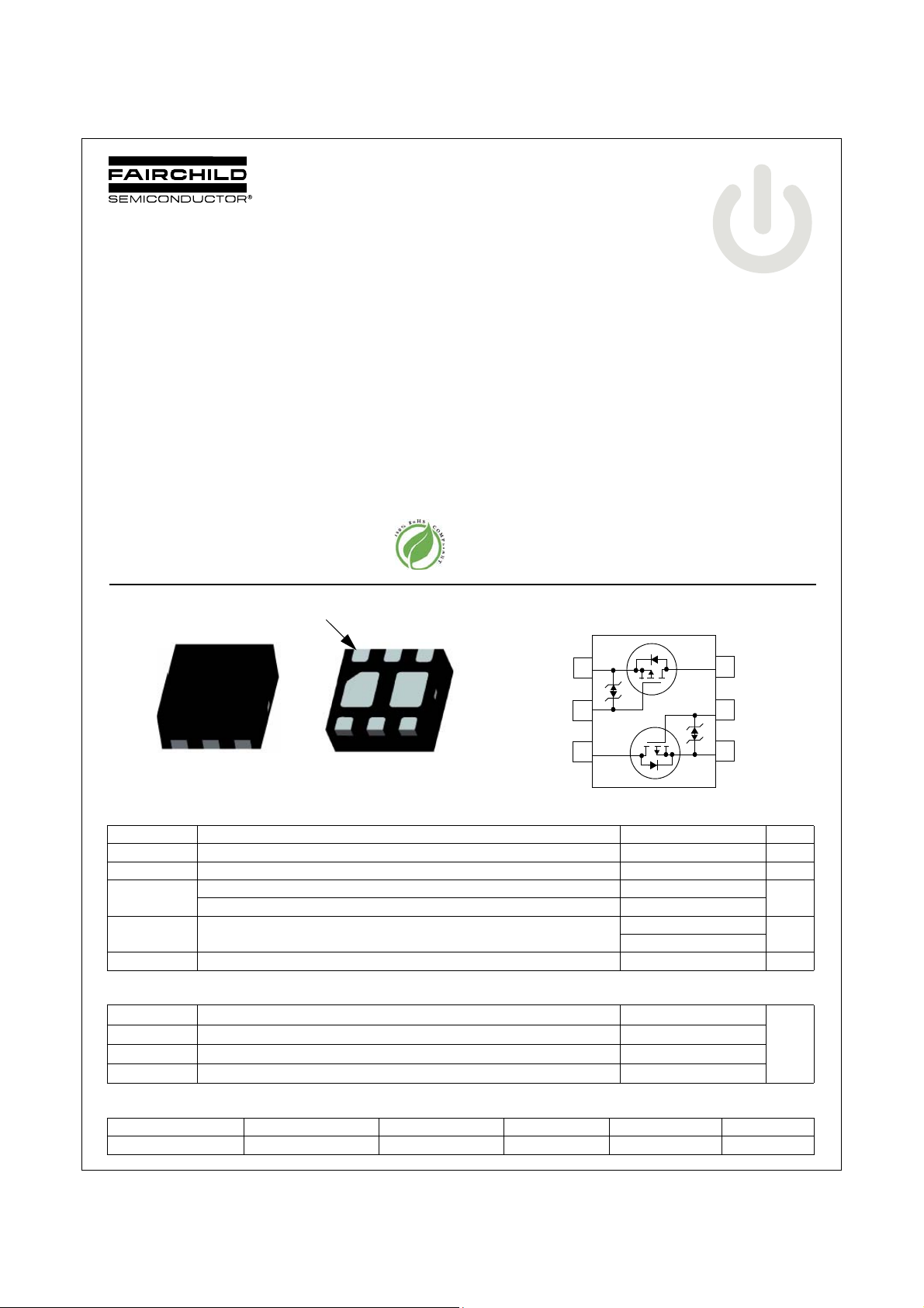
Pin 1
G1
D2
S2
D2
S1
G1
D2
6
1
2
3
1.5
0.7
D1
G2
5
4
S2
S1
D1
D1
MicroFET 2X2
MOSFET Maximum Ratings T
Symbol Parameter Ratings Units
V
DS
V
GS
I
D
P
D
, T
T
J
STG
Drain to Source Voltage –20 V
Gate to Source Voltage ±8 V
Drain Current -Continuous (Note 1a) –3.7
-Pulsed –6
Power Dissipation (Note 1a)
(Note 1b)
Operating and Storage Junction Temperature Range –55 to +150 °C
G2
= 25°C unless otherwise noted
A
Thermal Characteristics
R
TJA
R
TJA
R
TJA
R
TJA
Thermal Resistance for Single Operation, Junction to Ambient (Note 1a) 86
Thermal Resistance for Single Operation, Junction to Ambient (Note 1b) 173
Thermal Resistance for Dual Operation, Junction to Ambient (Note 1c) 69
Thermal Resistance for Dual Operation, Junction to Ambient (Note 1d) 151
Package Marking and Ordering Information
A
W
°C/W
Device Marking Device Package Reel Size Tape Width Quantity
023 FDMA1023PZ MicroFET 2X2 7” 8mm 3000 units
©2009 Fairchild Semiconductor Corporation
FDMA1023PZ Rev.C3
1
www.fairchildsemi.com

FDMA1023PZ Dual P-Channel PowerTrench
Electrical Characteristics T
= 25°C unless otherwise noted
J
Symbol Parameter Test Conditions Min Typ Max Units
Off Characteristics
BV
'BV
'T
I
DSS
I
GSS
DSS
DSS
J
Drain to Source Breakdown Voltage ID = –250PA, VGS = 0V –20 V
Breakdown Voltage Temperature
Coefficient
I
= –250PA, referenced to 25°C –11 mV/°C
D
Zero Gate Voltage Drain Current VDS = –16V, VGS= 0V –1 PA
Gate to Source Leakage Current VGS = ±8V, VDS= 0V ±10 PA
On Characteristics
V
GS(th)
'V
'T
r
DS(on)
g
FS
GS(th)
J
Gate to Source Threshold Voltage VGS = VDS, ID = –250PA –0.4 –0.7 –1.0 V
Gate to Source Threshold Voltage
Temperature Coefficient
Static Drain to Source On-Resistance
= –250PA, referenced to 25°C 2.5 mV/°C
I
D
V
= –4.5V, ID = –3.7A 60 72
GS
= –2.5V, ID = –3.2A 75 95
V
GS
= –1.8V, ID = –2.0A 100 130
V
GS
= –1.5V, ID = –1.0A 130 195
V
GS
= –4.5V, ID = –3.7A,TJ =125°C 81 91
V
GS
Forward Transconductance VDS = –5V, ID = –3.7A 12 S
Dynamic Characteristics
C
iss
C
oss
C
rss
Input Capacitance
Output Capacitance 100 135 pF
Reverse Transfer Capacitance 90 135 pF
= –10V, VGS = 0V,
V
DS
f = 1MHz
490 655 pF
m:
®
MOSFET
Switching Characteristics
t
d(on)
t
r
t
d(off)
t
f
Q
Q
Q
g(TOT)
gs
gd
Turn-On Delay Time
Rise Time 12 22 ns
Turn-Off Delay Time 64 103 ns
Fall Time 37 60 ns
Total Gate Charge
Gate to Source Gate Charge 0.7 nC
Gate to Drain “Miller” Charge 2.0 nC
Drain-Source Diode Characteristics
I
S
V
SD
t
rr
Q
rr
Maximum Continuous Source-Drain Diode Forward Current
Source to Drain Diode Forward Voltage VGS= 0V, IS= –1.1A (Note 2) –0.8 –1.2 V
Reverse Recovery Time
Reverse Recovery Charge 15 23 nC
VDD = –10V, ID = –1A
= –4.5V, R
V
GS
V
= –10V, ID = –3.7A
DD
= –4.5V
V
GS
= –3.7A, di/dt = 100A/Ps
I
F
GEN
= 6:
918ns
8.6 12 nC
–1.1 A
32 48 ns
FDMA1023PZ Rev.C3
2
www.fairchildsemi.com

Notes:
1: R
is determined with the device mounted on a 1 in2 oz. copper pad on a 1.5 x 1.5 in. board of FR-4 material. R
TJA
user's board design.
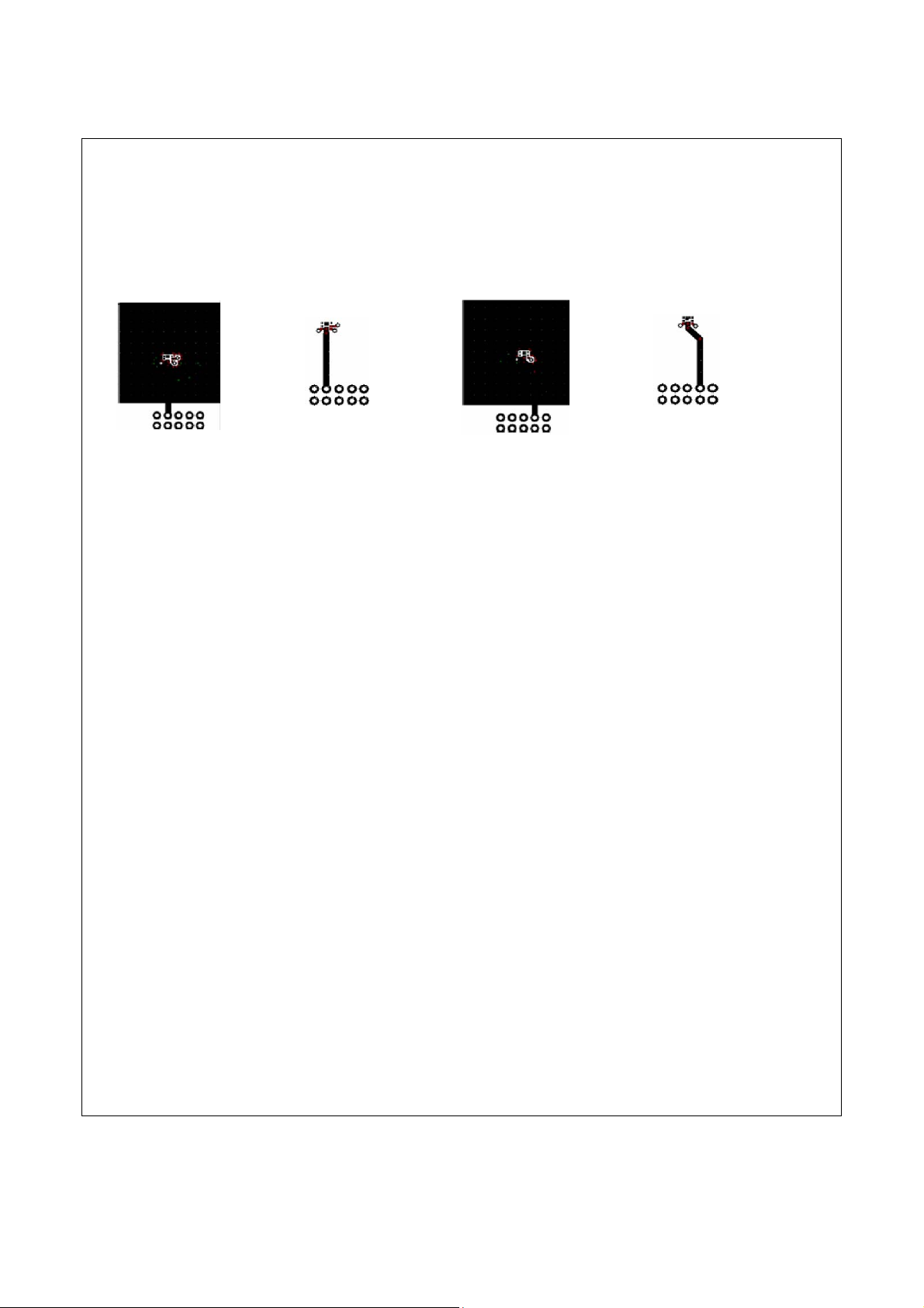
(a) R
= 86°C/W when mounted on a 1in2 pad of 2 oz copper, 1.5" x 1.5" x 0.062" thick PCB. For single operation.
TJA
(b) R
= 173°C/W when mounted on a minimum pad of 2 oz copper. For single operation.
TJA
(c) R
(d) R
= 69oC/W when mounted on a 1in2pad of 2 oz copper, 1.5” x 1.5” x 0.062” thick PCB, For dual operation.
TJA
= 151oC/W when mounted on a minimum pad of 2 oz copper. For dual operation.
TJA
is guaranteed by design while R
TJC
is determined by the
TJA
FDMA1023PZ Dual P-Channel PowerTrench
o
C/W when
a) 86oC/W when
mounted on a
2
1 i n
pad of 2
oz copper.
2: Pulse Test : Pulse Width < 300us, Duty Cycle < 2.0%
3: The diode connected between the gate and source serves only as protection against ESD. No gate overvoltage rating is implied.
b) 173
mounted on a
mini mum pad of
2 oz copper.
o
c) 69
C/W when
mounted on a
2
1 in
pad of 2
oz copper.
o
C/W when
d) 151
mounted on a
minimum pad of
2 oz copper.
®
MOSFET
FDMA1023PZ Rev.C3
3
www.fairchildsemi.com
 Loading...