tm
FDM3622
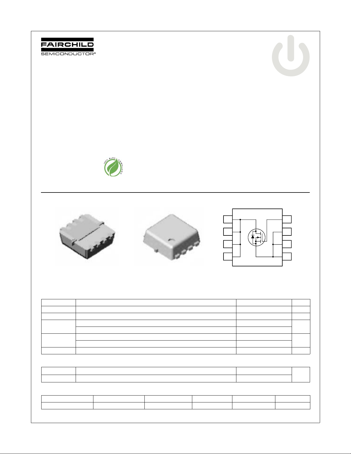
N-Channel PowerTrench® MOSFET
100V, 4.4A, 60mΩ
Features
Max r
Max r
Low Miller Charge
Low QRR Body Diode
Optimized efficiency at high frequencies
UIS Capability (Single Pulse and Repetitive Pulse)
RoHS Compliant
= 60mΩ at VGS = 10V, ID = 4.4A
DS(on)
= 80mΩ at VGS = 6.0V, ID = 3.8A
DS(on)
General Description
This N-Channel MOSFET is produced using Fairchild
Semiconductor's advanced PowerTrench
been especially tailored to minimize the on-state resistance and
yet maintain low gate charge for superior switching performance.
Application
Distributed Power Architectures and VRMs.
Primary Switch for 24V and 48V Systems
High Voltage Synchronous Rectifier
Formerly developmental type 82744
January 2007
®
process that has
FDM3622 N-Channel PowerTrench
®
MOSFET
Bottom
8
7
6
5
1
2
3
4
D
D
Top
D
D
D
5
D
6
D
7
G
S
S
S
D
8
Power 33
MOSFET Maximum Ratings T
Symbol Parameter Ratings Units
V
DS
V
GS
I
D
P
D
, T
T
J
STG
Drain to Source Voltage 100 V
Gate to Source Voltage ±20 V
Drain Current -Continuous (Note 1a) 4.4
-Pulsed 20
Power Dissipation (Note 1a) 2.1
Power Dissipation (Note 1b) 0.9
Operating and Storage Junction Temperature Range -55 to +150 °C
= 25°C unless otherwise noted
A
Thermal Characteristics
G
4
S
3
S
2
S
1
A
W
R
θJC
R
θJA
Thermal Resistance, Junction to Case (Note 1) 3.0
Thermal Resistance, Junction to Ambient (Note 1a) 60
Package Marking and Ordering Information
Device Marking Device Package Reel Size Tape Width Quantity
FDM3622 FDM3622 Power 33 7’’ 8mm 3000 units
©2006 Fairchild Semiconductor Corporation
FDM3622 Rev.B
°C/W
1
www.fairchildsemi.com

FDM3622 N-Channel PowerTrench
Electrical Characteristics T
= 25°C unless otherwise noted
J
Symbol Parameter Test Conditions Min Typ Max Units
Off Characteristics
BV
DSS
I
DSS
I
GSS
On Characteristics
V
GS(th)
r
DS(on)
Drain to Source Breakdown Voltage ID = 250μA, VGS = 0V 100 V
Zero Gate Voltage Drain Current
Gate to Source Leakage Current VGS = ±20V, V
VDS = 80V, VGS = 0V 1
TJ = 100°C 250
= 0V ±100 nA
DS
Gate to Source Threshold Voltage VGS = VDS, ID = 250μA 2 4 V
VGS = 10V, ID = 4.4A 44 60
Static Drain to Source On Resistance
VGS = 10V, ID = 4.4A , TJ = 150°C 92 120
Dynamic Characteristics
C
iss
C
oss
C
rss
Rg Gate Resistance VDS = 15mV, f = 1MHz 3.1 Ω
Input Capacitance
Output Capacitance 125 170 pF
Reverse Transfer Capacitance 35 55 pF
VDS = 25V, VGS = 0V,
f = 1MHz
820 1090 pF
Switching Characteristics
t
d(on)
t
r
t
d(off)
t
f
Q
Q
Q
g
gs
gd
Turn-On Delay Time
Rise Time 25 40 ns
Turn-Off Delay Time 35 56 ns
VDD = 50V, ID = 4.4A
VGS = 10V, R
GEN
= 24Ω
11 20 ns
Fall Time 26 42 ns
Total Gate Charge V
Gate to Source Gate Charge 3.6 nC
Gate to Drain “Miller” Charge 3.4 nC
= 10V
GS
VDD = 50V
ID = 4.4A
13 17 nC
μA
mΩVGS = 6.0V, ID = 3.8A 56 80
®
MOSFET
Drain-Source Diode Characteristics
V
SD
t
rr
Q
rr
Notes:
1: R
θJA
user's board design.
(a)R
θJA
(b)R
θJA
2: Pulse Test: Pulse Width < 300μs, Duty cycle < 2.0%.
FDM3622 Rev.B
Source to Drain Diode Forward Voltage
Reverse Recovery Time
Reverse Recovery Charge 108 nC
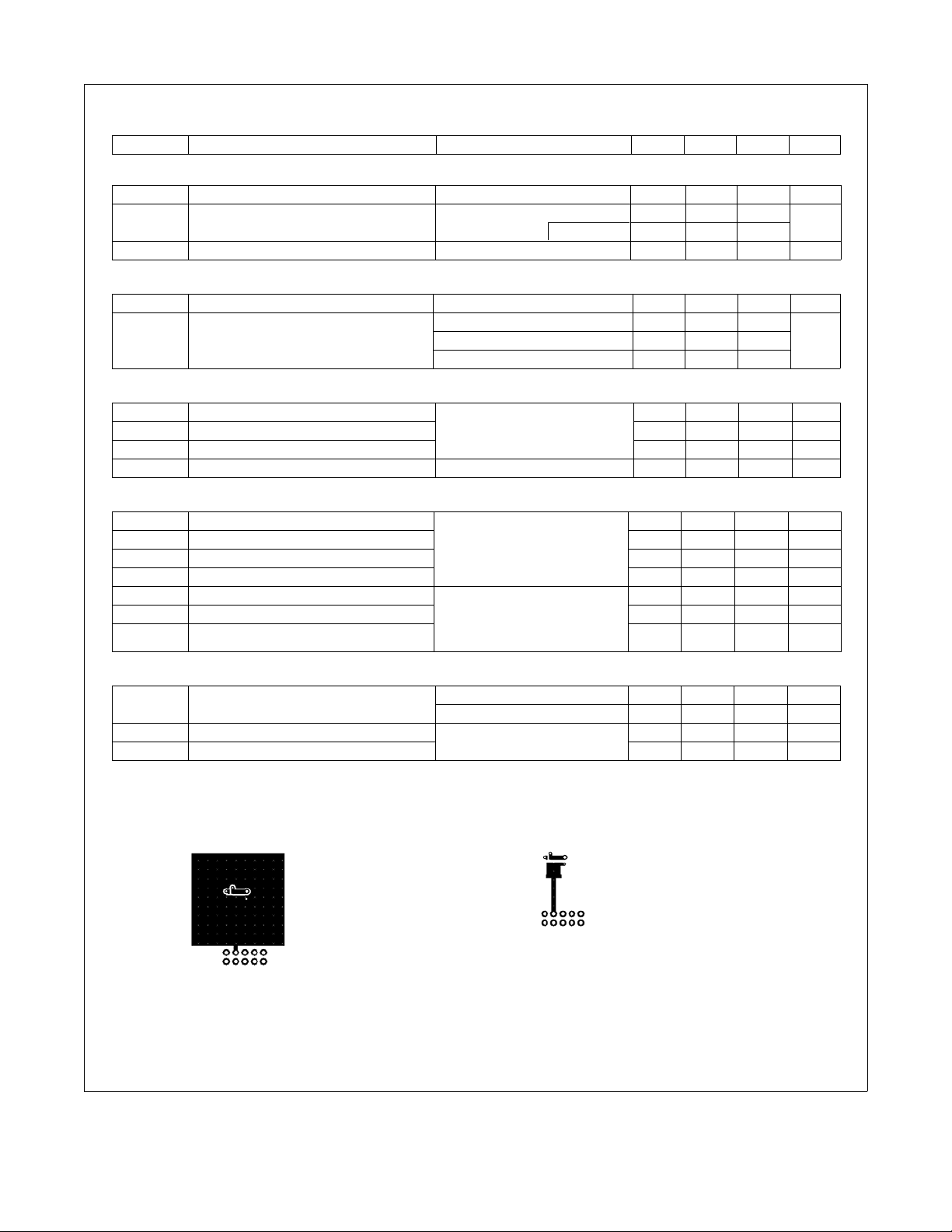
is determined with the device mounted on a 1 in2 oz copper pad on a 1.5 x 1.5 in. board of FR-4 material. R
= 60°C/W when mounted on a 1 in2 pad of 2 oz copper, 1.5’x1.5’x0.062’ thick PCB.
= 135°C/W when mounted on a minimum pad of 2 oz copper.
V
V
IF = 4.4A, di/dt = 100A/μs
a. 60°C/W when mounted on
2
pad of 2 oz copper
a 1 in
= 0V, IS = 4.4A 1.25 V
GS
= 0V, IS = 2.2A 1.0 V
GS
56 ns
is guaranteed by design while R
θJC
b. 135°C/W when mounted on a
minimum pad of 2 oz copper
2
is determined by the
θJA
www.fairchildsemi.com

FDM3622 N-Channel PowerTrench
Typical Characteristics T
10
VGS = 10V
8
6
4
, DRAIN CURRENT (A)
D
I
2
0
0 0.5 1.0 1.5 2.0 2.5 3.0
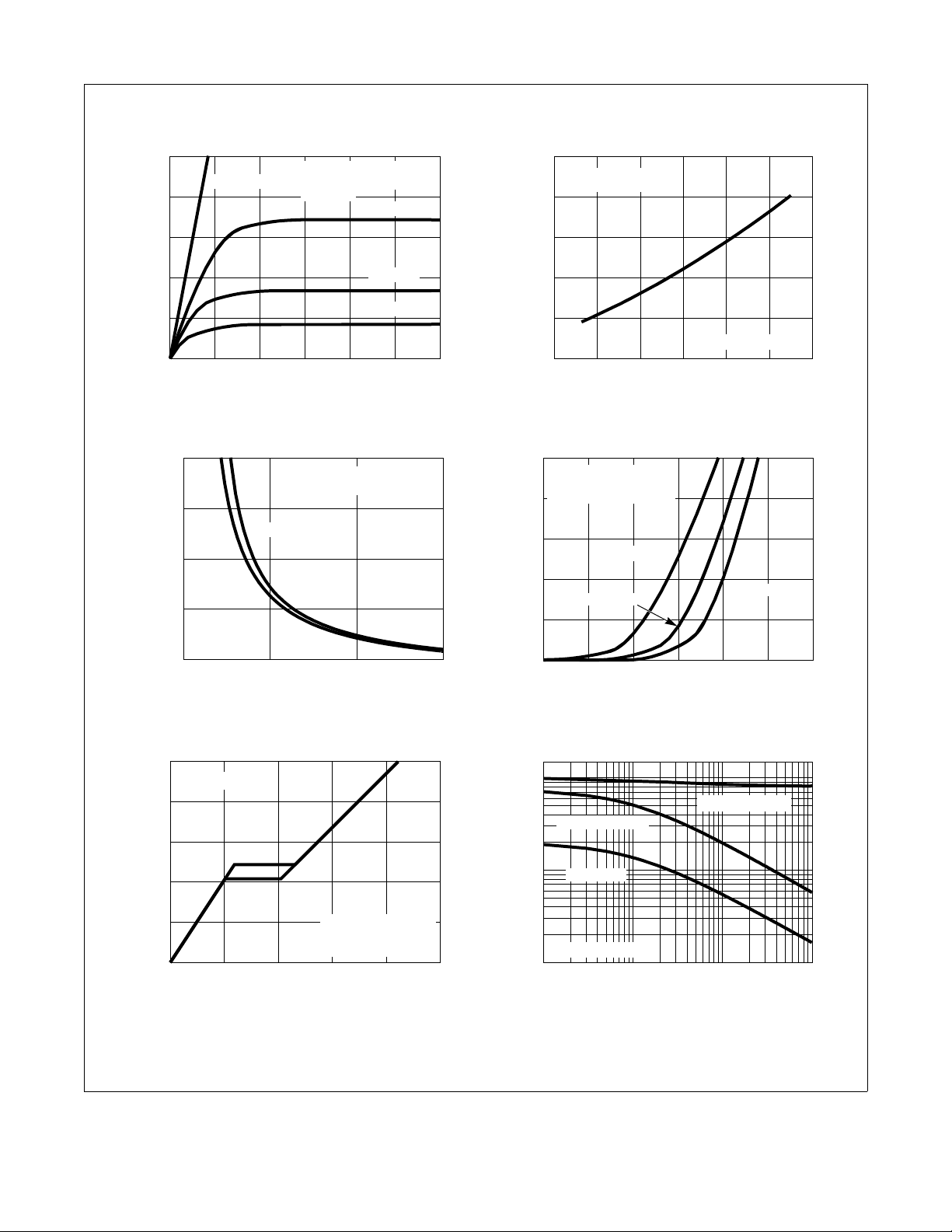
Figure 1.
80
70
60
, DRAIN TO SOURCE
ON RESISTANCE (mΩ)
50
DS(ON)
r
VDS, DRAIN TO SOURCE VOLTAGE (V)
On-Region Characteristics Figure 2.
ID = 4.4A
ID = 0.2A
PULSE DURATION = 80μs
DUTY CYCLE = 0.5% MAX
TA = 25oC
= 25°C unless otherwise noted
J
VGS = 5V
VGS = 4.7V
VGS = 4.5V
PULSE DURATION = 80μs
DUTY CYCLE = 0.5% MAX
2.5
PULSE DURATION = 80μs
DUTY CYCLE = 0.5% MAX
2.0
1.5
1.0
ON RESISTANCE
0.5
NORMALIZED DRAIN TO SOURCE
0
-80 -40 0 40 80 120 160
TJ, JUNCTION TEMPERATURE (oC)
VGS = 10V, ID = 4.4A
Normali z e d O n - R esistance
vs Junction Temperature
10
PULSE DURATION = 80μs
DUTY CYCLE = 0.5% MAX
V
= 15V
DD
8
, DRAIN CURRENT (A)
D
I
6
4
2
TJ = 150oC
TJ = 25oC
TJ = -55oC
®
MOSFET
10
8
6
4
2
, GATE TO SOURCE VOLTAGE (V)
GS
V
0
FDM3622 Rev.B
40
468
, GATE TO SOURCE VOLTAGE (V)
V
GS
10
Figure 3. On-Re sistance vs G ate to
Source Voltage
VDD = 50V
WAVEFORMS IN
DESCENDING ORDER:
ID = 4.4A
ID = 1A
03691215
Figure 5.
Qg, GATE CHARGE (nC)
Gate Charge Characteristics Figure 6. Capacitance vs Drain
0
3.0 3.5 4.0 4.5 5.0 5.5 6.0
1200
1000
100
C, CAPACITANCE (pF)
10
0.1 1 10 100
3
VGS, GATE TO SOURCE VOLTAGE (V)
Figure 4. Transfer Characteristics
C
= CGS + C
ISS
C
≅ C
+ C
OSS
DS
GD
C
= C
RSS
GD
V
= 0V, f = 1MHz
GS
VDS, DRAIN TO SOURCE VOLTAGE (V)
to Source Voltage
www.fairchildsemi.com
GD
 Loading...