

FDP038AN06A0 / FDI038AN06A0
N-Channel PowerTrench® MOSFET
60V, 80A, 3.8mΩ
FDP038AN06A0 / FDI038AN06A0
December 2010
Features
•r
•Q
• Low Miller Charge
•Low Q
• UIS Capability (Single Pulse and Repetitive Pulse)
= 3.5mΩ (Typ.), V
DS(ON)
(tot) = 95nC (Typ.), V
g
Body Diode
RR
= 10V, ID = 80A
GS
= 10V
GS
Applications
• Motor / Body Load Control
•ABS Systems
• Powertrain Management
• Injection Systems
• DC-DC converters and Off-line UPS
• Distributed Power Architectures and VRMs
Formerly developme ntal type 82584
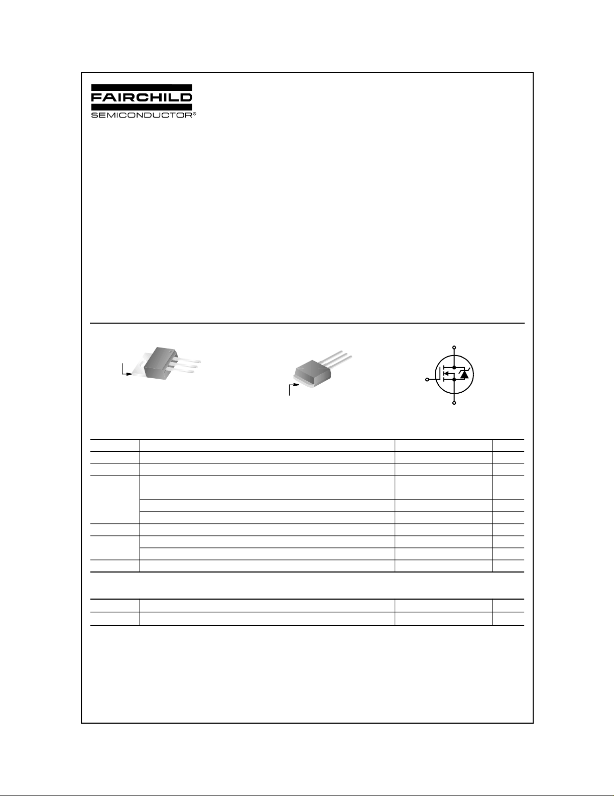
DRAIN
(FLANGE)
SOURCE
DRAIN
GATE
TO-220AB
FDP SERIES
MOSFET Maximum Ratings T
DRAIN
(FLANGE)
= 25°C unless otherwise noted
C
• Primary Switch for 12V and 24V systems
SOURCE
TO-262AB
FDI SERIES
DRAIN
GATE
D
G
S
Symbol Parameter Ratings Units
V
DSS
V
GS
Drain to Source Voltage 60 V
Gate to Source Voltage ±20 V
Drain Current
I
D
Continuous (T
Continuous (T
< 151oC, VGS = 10V)
C
= 25oC, VGS = 10V, with R
amb
= 62oC/W) 17 A
θJA
80 A
Pulsed Figure 4 A
E
AS
P
D
, T
T
J
STG
Single Pulse Avalanche Energy (Note 1) 625 mJ
Power dissipation 310 W
o
Derate above 25
C2.07W/
Operating and Storage Temperature -55 to 175
o
C
o
C
Thermal Characteristics
R
θJC
R
θJA
©2010 Fairchild Semiconductor Corporation
Thermal Resistance Junction to Case TO-220, TO-262 0.48
Thermal Resistance Junction to Ambient TO-220, TO-262 (Note 2) 62
o
C/W
o
C/W
FDP038AN06A0 / FDI038AN06A0 Rev. B2
Package Marking and Ordering Information
Device Marking Device Package Reel Size Tape Width Quantity
FDP038AN06A0 FDP038AN06A0 TO-220AB Tube N/A 50 units
FDI038AN06A0 FDI038AN06A0 TO-262AB Tube N/A 50 units
FDP038AN06A0 / FDI038AN06A0
Electrical Characteristics
TC = 25°C unless otherwise noted
Symbol Parameter Tes t Cond itions Min Typ Max Units
Off Characteristics
B
I
DSS
I
GSS
VDSS
Drain to Source Breakdown Volt age ID = 250µA, VGS = 0V 60 - - V
V
= 50V - - 1
Zero Gate Voltage Drain Current
DS
= 0V TC = 150oC - - 250
V
GS
Gate to Source Leakage Current VGS = ±20V - - ±100 nA
On Characteristics
V
GS(TH)
r
DS(ON)
Gate to Source Threshold Voltage VGS = VDS, ID = 250µA2-4V
= 80A, VGS = 10V - 0.0035 0.0038
I
D
I
= 40A, VGS = 6V - 0.0049 0.0074
Drain to Source On Resistance
D
= 80A, VGS = 10V,
I
D
T
= 175oC
J
- 0.0071 0.0078
Dynamic Characteristics
C
C
C
Q
Q
Q
Q
Q
ISS
OSS
RSS
g(TOT)
g(TH)
gs
gs2
gd
Input Capacitance
Output Capacitance - 1123 - pF
Reverse Transfer Capacitance - 367 - pF
= 25V, VGS = 0V,
V
DS
f = 1MHz
Total Gate Charge at 10V VGS = 0V to 10V
Threshold Gate Charge VGS = 0V to 2V - 12 15 nC
Gate to Source Gate Charge - 26 - nC
Gate Charge Threshold to Plateau - 15 - nC
V
DD
= 80A
I
D
= 1.0mA
I
g
= 30V
Gate to Drain “Miller” Charge - 27 - nC
- 6400 - pF
96 124 nC
µA
Ω
Switching Characteristics
t
ON
t
d(ON)
t
r
t
d(OFF)
t
f
t
OFF
Turn-On Time
Turn-On Delay Time - 17 - ns
Rise Time - 144 - ns
Tur n-Off Delay Time - 34 - ns
Fall Time - 60 - n s
Turn-Off Time - - 115 ns
(VGS = 10V)
= 30V, ID = 80A
V
DD
= 10V, RGS = 2.4Ω
V
GS
- - 175 ns
Drain-Source Diode Characteristics
I
= 80A - - 1.25 V
V
SD
t
rr
Q
RR
Notes:
1: Starting T
2: Pulse Width = 100s
©2010 Fairchild Semiconductor Corporation FDP038AN06A0 / FDI038AN06A0 Rev. B2
Source to Drain Diode Voltage
Reverse Recovery Time ISD = 75A, dISD/dt = 100A/µs- -38ns
Reverse Recovered Charge ISD = 75A, dISD/dt = 100A/µs- -39nC
= 25°C, L = 0.255mH, IAS = 70A.
J
SD
= 40A - - 1.0 V
I
SD
FDP038AN06A0 / FDI038AN06A0
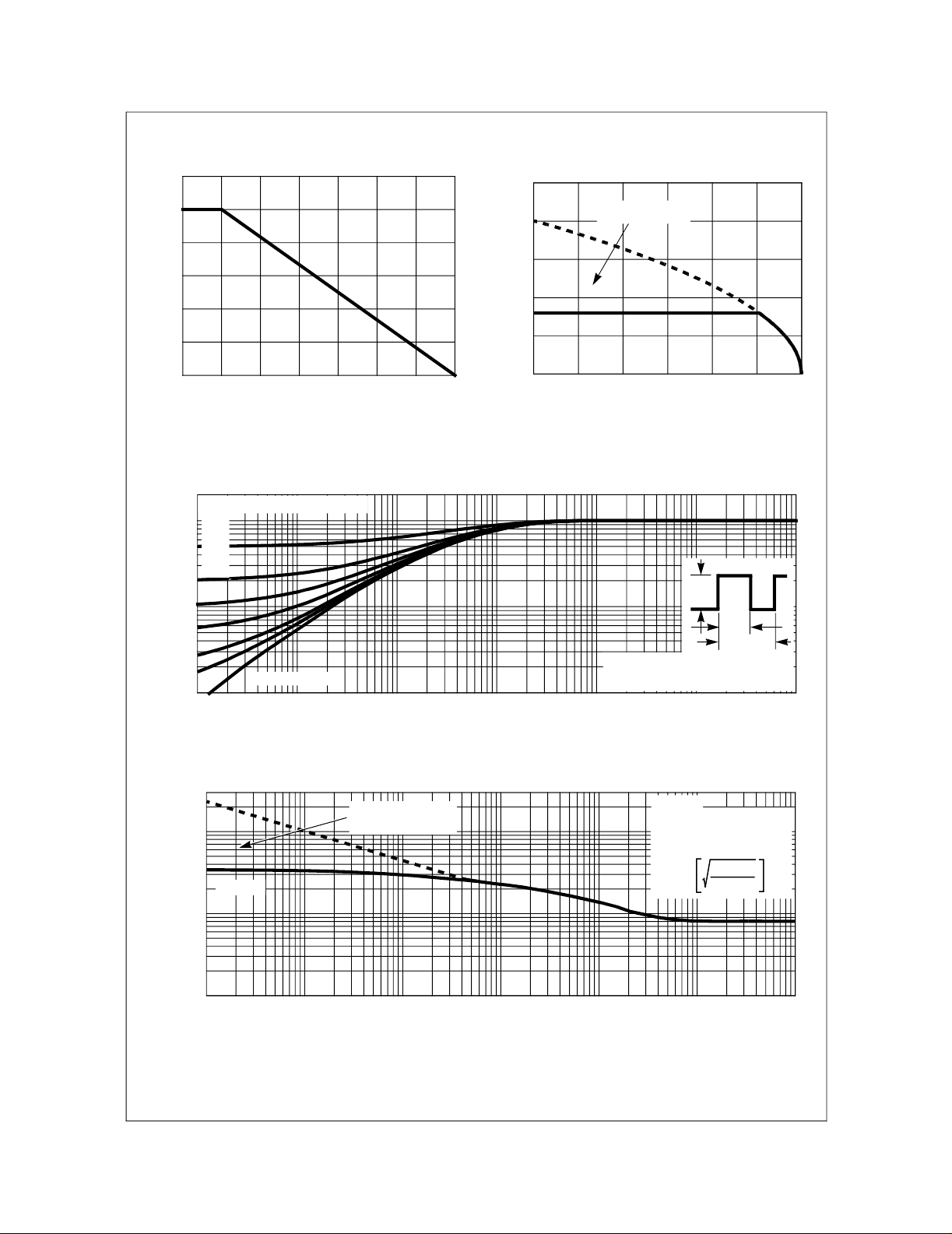
Typical Characteristics T
1.2
1.0
0.8
0.6
0.4
0.2
POWER DISSIPATION MULTIPLIER
0
0 25 50 75 100 175
TC, CASE TEMPERATURE (oC)
= 25°C unless otherwise noted
C
125
Figure 1. Normalized Power Dissipation vs
Ambient Temperature
2
DUTY CYCLE - DESCENDING ORDER
0.5
1
0.2
0.1
0.05
0.02
0.01
0.1
, NORMALIZED
θJC
Z
THERMAL IMPEDANCE
0.01
-5
10
SINGLE PULSE
-4
10
10
250
200
150
100
, DRAIN CURRENT (A)
D
I
50
0
150
25 50 75 100 125 150 175
Figure 2. Maximum Contin uous Drain Current vs
-3
t, RECTANGULAR PULSE DURATION (s)
-2
10
CURRENT LIMITED
BY PACKAGE
TC, CASE TEMPERATURE (oC)
Case Temperature
P
DM
NOTES:
DUTY FACTOR: D = t
PEAK TJ = PDM x Z
-1
10
1/t2
θJC
0
10
x R
θJC
t
+ T
1
t
2
C
1
10
Figure 3. Normalized Maximum Transient Thermal Impedance
3000
TRANSCONDUCTANCE
MAY LIMIT CURRENT
-4
IN THIS REGION
-3
10
-2
10
t, PULSE WIDT H (s)
-1
10
1000
VGS = 10V
100
, PEAK CURRENT (A)
DM
I
10
-5
10
10
TC = 25oC
FOR TEMPERATURES
o
ABOVE 25
CURRENT AS FOLLOWS:
I = I
25
C DERATE PEAK
175 - T
150
0
10
C
1
10
Figure 4. Peak Current Capability
©2010 Fairchild Semiconductor Corporation FDP038AN06A0 / FDI038AN06A0 Rev. B2

FDP038AN06A0 / FDI038AN06A0
Typical Characteristics T
2000
1000
100
OPERATION IN THIS
AREA MAY BE
10
LIMITED BY r
, DRAIN CURRENT (A)
D
I
1
SINGLE PULSE
TJ = MAX RATED
T
= 25oC
C
0.1
110100
Figure 5. Forward Bias Safe Operating Area
160
PULSE DURATION = 80µs
DUTY CYCLE = 0.5% MAX
V
DD
120
DS(ON)
VDS, DRAIN TO SOURCE VOLTAGE (V)
= 15V
= 25°C unless otherwise noted
C
10µs
100µs
1ms
10ms
DC
NOTE: Refer to Fairchild Applica tion N ote s AN7514 and AN7515
100
STARTING TJ = 25oC
STARTING TJ = 150oC
10
, AVALANCHE CURRENT (A)
I
If R = 0
tAV = (L)(IAS)/(1.3*RATED BV
AS
If R ≠ 0
t
= (L/R)ln[(IAS*R)/(1.3*RATED BV
AV
1
0.01 0.1 1 10 100
tAV, TIME IN AVALANCHE (ms)
DSS
- VDD)
DSS
- VDD) +1]
Figure 6. Unclamped Inductive Switching
Capability
160
120
VGS = 20V
VGS = 6V
VGS = 10V
VGS = 5V
80
, DRAIN CURRENT (A)
D
I
40
0
3.0 3.5 4.0 4.5 5.0 5.5 6
TJ = 175oC
TJ = 25oC
TJ = -55oC
VGS, GATE TO SOURCE VOLTAGE (V)
Figure 7. Transfer Ch aracteri stics Figur e 8. Satura tion Characteristics
6
PULSE DURATION = 80µs
DUTY CYCLE = 0.5% MAX
5
4
DRAIN TO SOURCE ON RESISTANCE(mΩ)
3
0 20406080
, DRAIN CURRENT (A)
I
D
VGS = 6V
VGS = 10V
Figure 9. Drain to Sour ce On Resistan ce vs Drain
Current
80
, DRAIN CURRENT (A)
D
I
40
PULSE DURATION = 80µs
0
0 0.5 1.0 1.5
2.5
PULSE DURATION = 80µs
DUTY CYCLE = 0.5% MAX
2.0
1.5
ON RESISTANCE
1.0
NORMALIZED DRAIN TO SOURCE
0.5
-80 -40 0 40 80 120 160 200
DUTY CYCLE = 0.5% MAX
VDS, DRAIN TO SOURCE VOLTAGE (V)
TJ, JUNCTION TEMPERATURE (oC)
TC = 25oC
VGS = 10V, ID =80A
Figure 10. Normalized Drain to Source On
Resistance vs Junction Temperature
©2010 Fairchild Semiconductor Corporation FDP038AN06A0 / FDI038AN06A0 Rev. B2

FDP038AN06A0 / FDI038AN06A0
Typical Characteristics T
1.4
1.2
1.0
0.8
0.6
NORMALIZED GATE
THRESHOLD VOLTAGE
0.4
0.2
-80 -40 0 40 80 120 160 200
TJ, JUNCTION TEMPERATURE (oC)
= 25°C unless otherwise noted
C
VGS = VDS, ID = 250µA
Figure 11. Normalized Gate Thresho ld Voltage vs
Junction Temperature
10000
C
= CGS + C
C
≅ C
+ C
OSS
DS
GD
1000
C, CAPACITANCE (pF)
C
= C
RSS
GD
V
= 0V, f = 1MHz
GS
100
0.1 1 10 60
VDS, DRAIN TO SOURCE VOLTAGE (V)
ISS
GD
1.2
ID = 250µA
1.1
1.0
BREAKDOWN VOLTAGE
NORMALIZED DRAIN TO SOURCE
0.9
-80 -40 0 40 80 120 160 200
TJ, JUNCTION TEMPERATURE (oC)
Figure 12. Normalized Drain to Source
Breakdown Voltage vs Junction Temperature
10
VDD = 30V
8
6
4
WAVEFORMS IN
2
, GATE TO SOURCE VOLTAGE (V)
GS
V
0
0 255075100
Qg, GATE CHARGE (nC)
DESCENDING ORDER:
ID = 80A
I
= 40A
D
Figure 13. Capacitance vs Drain to Source
Voltage
©2010 Fairchild Semiconductor Corporation FDP038AN06A0 / FDI038AN06A0 Rev. B2
Figure 14. Gate Charge Waveforms for Constant
Gate Current

Test Circuits and Waveforms
V
DS
L
TO OBTAIN
VARY t
P
REQUIRED PEAK I
V
GS
R
AS
G
+
V
DD
-
I
AS
DUT
t
0V
P
I
AS
0.01Ω
0
Figure 15. Unclamped Energy Test Circuit Figure 16. Unclamped Energy Waveforms
BV
DSS
t
P
t
AV
FDP038AN06A0 / FDI038AN06A0
V
DS
V
DD
V
DS
I
g(REF)
V
DD
L
V
GS
DUT
+
V
DD
-
V
GS
0
I
g(REF)
= 2V
Q
gs2
Q
g(TH)
Q
gs
Q
g(TOT)
V
DS
Q
gd
V
0
Figure 17. Gate Charge Test Circuit Figure 18. Gate Charge Waveforms
V
DS
R
L
V
GS
R
GS
V
GS
DUT
+
V
DD
-
V
DS
0
V
GS
10%
0
t
d(ON)
90%
t
ON
50%
10%
t
r
PULSE WIDTH
GS
t
d(OFF)
V
= 10V
GS
t
OFF
t
f
90%
10%
90%
50%
Figure 19. Switching Time Test Circuit Figure 20. Switching Time Waveforms
©2010 Fairchild Semiconductor Corporation FDP038AN06A0 / FDI038AN06A0 Rev. B2

PSPICE Electrical Model
.SUBCKT FDP038AN06A0 2 1 3 ; rev July 04, 2002
Ca 12 8 1.5e-9
Cb 15 14 1.5e-9
Cin 6 8 6.1e-9
Dbody 7 5 DbodyMOD
Dbreak 5 11 DbreakMOD
Dplcap 10 5 DplcapMOD
Ebreak 11 7 17 18 69.3
Eds 14 8 5 8 1
Egs 13 8 6 8 1
Esg 6 10 6 8 1
Evthres 6 21 19 8 1
Evtemp 20 6 18 22 1
It 8 17 1
Lgate 1 9 4.81e-9
Ldrain 2 5 1.0e-9
Lsource 3 7 4.63 e -9
RLgate 1 9 48.1
RLdrain 2 5 10
RLsource 3 7 46.3
Mmed 16 6 8 8 MmedMOD
Mstro 16 6 8 8 MstroMOD
Mweak 16 21 8 8 MweakMOD
Rbreak 17 18 RbreakMOD 1
Rdrain 50 16 RdrainMOD 1e-4
Rgate 9 20 1.36
RSLC1 5 51 RSLCMOD 1e-6
RSLC2 5 50 1e3
Rsource 8 7 RsourceMOD 2.8e-3
Rvthres 22 8 RvthresMOD 1
Rvtemp 18 19 RvtempMOD 1
S1a 6 12 13 8 S1AMOD
S1b 13 12 13 8 S1BMOD
S2a 6 15 14 13 S2AMOD
S2b 13 15 14 13 S2BMOD
GATE
1
LGATE
RLGATE
RGATE
9
CA
ESG
+
EVTEMP
+
-
18
22
20
S1A
12
13
8
S1B
EGS EDS
-
13
6
8
10
RSLC2
6
14
13
+
+
6
8
-
-
DPLCAP
EVTHRES
+
S2A
S2B
5
RSLC1
51
+
5
51
50
RDRAIN
21
-
19
8
MSTRO
CIN
15
CB
14
+
5
8
-
ESLC
16
8
MMED
8
DBREAK
11
+
17
EBREAK
IT
18
-
MWEAK
RSOURCE
RBREAK
17 18
RVTHRES
7
+
RVTEMP
19
-
22
LDRAIN
RLDRAIN
DBODY
LSOURCE
RLSOURCE
VBAT
DRAIN
2
SOURCE
3
FDP038AN06A0 / FDI038AN06A0
Vbat 22 19 DC 1
ESLC 51 50 VALUE={(V(5,51)/ABS(V(5,51)))*(PWR(V(5,51)/(1e-6*250),10))}
.MODEL DbodyMOD D (IS=2.4E-11 N=1.04 RS=1.65e-3 TRS1=2.7e-3 TRS2=2e-7
+ CJO=4.35e-9 M=5.4e-1 TT=1e-9 XTI=3.9)
.MODEL DbreakMOD D (RS=1.5e-1 TRS1=1e-3 TRS2=-8.9e-6)
.MODEL DplcapMOD D (CJO=1. 7e-9 IS=1e-30 N =1 0 M=0.47)
.MODEL MmedMOD NMOS (VTO=3.3 KP=9 IS=1e-30 N=10 TOX=1 L=1u W=1u RG=1.36 T_abs=25)
.MODEL MstroMOD NMOS (VTO=4.00 KP=275 IS=1e-30 N=10 TOX=1 L=1u W=1u T_abs=25)
.MODEL MweakMOD NMOS (VTO=2.72 KP=0.03 IS=1e-30 N=10 TOX=1 L=1u W=1u RG=13.6 RS=0.1 T_abs=25)
.MODEL RbreakMOD RES (TC1=9e-4 TC2=-9e-7)
.MODEL RdrainMOD RES (TC1=4e-2 TC2=3e-4 )
.MODEL RSLCMOD RES (TC1=1e -3 TC2=1e-5)
.MODEL RsourceMOD RES (TC1=5e-3 TC2=1e-6)
.MODEL RvthresMOD RES (TC1=-6.7e-3 TC2=-1.5e-5)
.MODEL RvtempMOD RES (TC1=- 2.5e-3 TC2=1e-6)
.MODEL S1AMOD VSWITCH (RON=1e-5 ROFF=0.1 VON=-4 VOFF=-1.5)
.MODEL S1BMOD VSWITCH (RON=1e-5 ROFF=0.1 VON=-1.5 VOFF=-4)
.MODEL S2AMOD VSWITCH (RON=1e-5 ROFF=0.1 VON=-1 VOFF=0.5)
.MODEL S2BMOD VSW ITCH (RON=1e-5 ROFF=0.1 VON=0.5 VOFF=-1)
.ENDS
Note: For further disc ussio n of the PSPI CE model, c onsult A New PSPICE Sub-Circuit for the Power MOSFET Featuring Global
Temperature Options; IEEE Power Electronics Specialist Conference Records, 1991, written by William J. Hepp and C. Frank
Wheatley.
©2010 Fairchild Semiconductor Corporation FDP038AN06A0 / FDI038AN06A0 Rev. B2

SABER Electrical Model
rev July 4, 2002
template FDP038AN06A0 n2,n1,n3 = m_temp
electrical n2,n1, n3
number m_temp=25
{
var i iscl
dp..model dbodymod = (isl=2.4e-11,nl=1.04,rs=1.65e-3,trs1=2.7e-3,trs2=2e-7,cjo=4.35e-9,m=5.4e-1,tt=1e-9,xti=3.9)
dp..model dbreakmod = (rs=1.5e-1,trs1=1e-3,trs2=-8.9e-6)
dp..model dplcapmod = (cjo=1.7e-9,isl=10e-30,nl=10,m=0.47)
m..model mmedmod = (type=_n,vto=3.3,kp=9,is=1e-30, tox=1)
m..model mstrong mod = (type=_n,vto=4.00,kp=275,is= 1e-30, tox=1)
m..model mweakmod = (type=_n,vto=2.72,kp=0.03,is=1e-30, tox=1,rs=0.1)
sw_vcsp..model s1amod = (ron=1e-5,roff=0.1,von=-4,voff=-1.5)
sw_vcsp..model s1bmod = (ron=1e-5,roff=0.1,von=-1.5,voff=-4)
sw_vcsp..model s2amod = (ron=1e-5,roff=0.1,von=-1,voff=0.5)
sw_vcsp..model s2bmod = (ron=1e-5,roff=0.1,von=0.5,voff=-1)
c.ca n12 n8 = 1.5e-9
c.cb n15 n14 = 1.5e-9
c.cin n6 n8 = 6.1e-9
dp.dbody n7 n5 = model=dbodymod
dp.dbreak n5 n11 = model=dbreakmod
dp.dplcap n10 n5 = model=dplcapmod
spe.ebreak n11 n7 n17 n18 = 69.3
GATE
spe.eds n14 n8 n5 n8 = 1
spe.egs n13 n8 n6 n8 = 1
LGATE
1
9
RLGATE
RGATE
ESG
EVTEMP
+
20
18
22
spe.esg n6 n10 n6 n8 = 1
spe.evthres n6 n21 n19 n8 = 1
spe.evtemp n20 n6 n18 n22 = 1
CA
S1A
12
S1B
i.it n8 n17 = 1
l.lgate n1 n9 = 4.81e-9
l.ldrain n2 n5 = 1.0e-9
l.lsource n3 n7 = 4.63e-9
res.rlgate n1 n9 = 48.1
res.rldrain n2 n5 = 10
res.rlsource n3 n7 = 46.3
m.mmed n16 n6 n8 n8 = model=mmedmod, temp=m_temp, l=1u, w=1u
m.mstrong n16 n6 n8 n8 = model=mstrongmod, temp=m_temp, l=1u, w=1u
m.mweak n16 n21 n8 n8 = model= mweakmod, temp=m_temp, l=1u, w=1u
res.rbreak n17 n18 = 1, tc1=9e-4,tc2=-9e - 7
res.rdrain n50 n16 = 1e-4, tc1=4e-2,tc2=3e-4
res.rgate n9 n20 = 1.3 6
res.rslc1 n5 n51 = 1e-6, tc1=1e-3,tc2=1 e-5
res.rslc2 n5 n50 = 1e3
res.rsource n8 n7 = 2.8e-3, tc1=5e-3,tc2=1e-6
res.rvthres n22 n8 = 1, tc1=-6.7e-3,tc2= -1.5e-5
res.rvtemp n18 n19 = 1, tc1=-2.5e-3,tc2=1e-6
sw_vcsp.s1a n6 n12 n13 n8 = model=s1amod
sw_vcsp.s1b n13 n12 n13 n8 = model=s1bmod
sw_vcsp.s2a n6 n15 n14 n13 = model=s2amod
sw_vcsp.s2b n13 n15 n14 n13 = model=s2bmod
DPLCAP
10
RSLC2
6
8
EVTHRES
+
+
19
8
6
-
S2A
14
13
13
8
S2B
13
+
+
6
EGS EDS
8
-
-
15
CIN
CB
-
+
-
5
51
21
MSTRO
14
5
8
RSLC1
ISCL
50
RDRAIN
16
8
MMED
8
DBREAK
11
MWEAK
EBREAK
+
-
RSOURCE
RBREAK
17 18
IT
RVTHRES
17
18
7
RVTEMP
19
-
+
22
RLSOURCE
LDRAIN
RLDRAIN
DBODY
LSOURCE
VBAT
DRAIN
2
SOURCE
3
FDP038AN06A0 / FDI038AN06A0
v.vbat n22 n19 = dc=1
equations {
i (n51->n50) +=iscl
iscl: v(n51,n50) = ((v(n 5,n51)/(1e-9+abs(v(n5,n51))))*((abs(v(n5,n51)*1e6/250))** 10))
}
©2010 Fairchild Semiconductor Corporation FDP038AN06A0 / FDI038AN06A0 Rev. B2

PSPICE Thermal Model
REV 23 July 4, 2002
FDP038AN06A0T
CTHERM1 TH 6 6. 45e-3
CTHERM2 6 5 3e-2
CTHERM3 5 4 1.4e-2
CTHERM4 4 3 1.65e-2
CTHERM5 3 2 4.85e-2
CTHERM6 2 TL 1e-1
RTHERM1 TH 6 3. 24e-3
RTHERM2 6 5 8.08e-3
RTHERM3 5 4 2.28e-2
RTHERM4 4 3 1e-1
RTHERM5 3 2 1.1e-1
RTHERM6 2 TL 1.4e-1
SABER Thermal Model
th
RTHERM1
6
RTHERM2
5
FDP038AN06A0 / FDI038AN06A0
JUNCTION
CTHERM1
CTHERM2
SABER thermal model FDP035AN06A0T
template thermal_model th tl
thermal_c th, tl
{
ctherm.ctherm1 t h 6 =6.45e-3
ctherm.ctherm2 6 5 =3e-2
ctherm.ctherm3 5 4 =1.4e-2
ctherm.ctherm4 4 3 =1.65e-2
ctherm.ctherm5 3 2 =4.85e-2
ctherm.ctherm6 2 tl =1e-1
rtherm.rtherm1 th 6 =3.24e-3
rtherm.rtherm2 6 5 =8.08e-3
rtherm.rtherm3 5 4 =2.28e-2
rtherm.rtherm4 4 3 =1e-1
rtherm.rtherm5 3 2 =1.1e-1
rtherm.rtherm6 2 tl=1.4 e-1
}
RTHERM3
RTHERM4
RTHERM5
RTHERM6
CTHERM3
4
CTHERM4
3
CTHERM5
2
CTHERM6
tl
CASE
©2010 Fairchild Semiconductor Corporation FDP038AN06A0 / FDI038AN06A0 Rev. B2

TRADEMARKS
The following
intended to be an exhaustive list of all such trademarks.
AccuPo
Auto-SPM™
Build it Now™
CorePLUS™
CorePOWER™
CROSSVOLT™
CTL™
Current Tr
DEUXPEED
Dual Co
EcoSPARK
E
fficentMax™
ESBC™
Fairchild
Fairchild Semi
FACT Qui
FACT
FAST
FastvCore™
FET
FlashWriter
FPS™
*Trademarks of System General Corporation, used under license by Fairchild Semiconductor.
DISCLAIMER
FAIRCHI
RELIABILITY, FUNCTION, OR DESIGN. FAIRCHILD DOES NOT ASSUME ANY LIABILITY ARISING OUT OF THE APPLICATION OR USE OF ANY
PRODUCT OR CIRCUIT DESCRIBED HEREIN; NEITHER DOES IT CONVEY ANY LICENSE UNDER ITS PATENT RIGHTS, NOR THE RIGHTS OF OTHERS.
THESE SPECIFICATIONS DO NOT EXPAND THE TERMS OF FAIRCHILD’S WORLDWIDE TERMS AND CONDITIONS, SPECIFICALLY THE WARRANTY
THEREIN, WHICH COVERS THESE PRODUCTS.
includes registered and unregistered trademarks and service marks, owned by Fairchild Semico nductor and/or its global subsidiaries, an d is not
wer™
ol™
®
®
et Series™
®
®
Bench™
ansfer Logic™
®
®
conductor
®
*
®
Series™
™
®
®
T™-3
®
®
The Power Franchise
The Right Te
TinyB
TinyBuck™
TinyCalc™
TinyLogic
TINYOPTO™
TinyPower™
Tin
TinyWire™
TriFault Detect™
TRUECURRENT™*
μSerD
UHC
Ultra
UniFET™
VCX™
VisualMax™
®
oost™
®
yPWM™
es™
®
FRFET™
XS™
F-PFS™
®
FRFET
Global Power
Green FPS™
Green FPS™
G
max™
GTO™
IntelliMAX
ISOPLANAR™
MegaBuck™
MICROCOUPLER™
MicroFET™
MicroPak™
MicroPak2™
MillerDrive™
®
MotionMax™
Motion-SPM™
OptiHiT™
OPTOLOGIC
OPTOP
®
™
LANAR
Resource
e-Series™
®
®
PDP SPM™
SPM™
Power-
PowerTrench
PowerXS™
SM
ogrammable Active Droop™
Pr
QFET
QS™
Quiet
RapidConfigure™
Saving our world, 1mW/W/kW at a time™
SignalWise™
SmartMax™
SMART START™
SPM
STEALTH™
Su
perFET
SuperSO
SuperSOT™-6
SuperSOT™-8
SupreMOS
SyncFET™
Sync-Lock™
®*
®
chnology for Y our Success™
LD SEMICONDUCTOR RESERVES THE RIGHT TO MAKE CHANGES WITHOUT FURTHER NOTICE TO ANY PRODUCTS HEREIN TO IMPROVE
FDP038AN06A0 / FDI038AN06A0
LIFE SUPPORT
FAIRCHIL
EXPRESS WRITTEN APPROVAL OF FAIRCHILD SEMICONDUCTOR CORPORATION.
POLICY
D’S PRODUCTS ARE NOT AUTHORIZED FOR USE AS CRITICAL COMPONENTS IN LIFE SUPPORT DEVICES OR SYSTEMS WITHOUT THE
As used here in:
1. Life support devices or syst ems are devices or syst ems which, (a) are
intended for surgical implant into the body or (b) support or sustain life,
and (c) whose failure to perform when properly used in accordance with
instructions for use provided in the labeling, can be reasonably
2. A critical component in any component of a life support, device, or
system whose failure to perform can be reasonably expected to cause
the failure of the life support device or system, or to affect its safety or
effectiveness.
expected to result in a significant injury of the user.
ANTI-COUNTERFEITING POLICY
Fairchild Semico
www.Fairchildsemi.com, under Sales Support
Counterfeiting of semiconductor pa
parts. Customers who inadvertently purchase counterfeit parts experience many problems such as loss of brand repu tation, su bsta ndard perfo rmance, failed
application, and increased cost of production and manufacturing delays. Fairchild is taking strong measures to pro tect ourselves and our customers from the
proliferation of counterfeit parts. Fairchild strongly encourages customers to purchase Fairchild parts eith er directly from Fa irchild or from Authorized Fairchild
Distributors who are listed by country on our web page cited above. Products customers buy either from Fairchild directly or from Authorized Fairchild
Distributors are genuine parts, have full traceability, meet Fairchild’s quality standards for handing and storage and provide access to Fairchild’s full range of
up-to-date technical and product information. Fairchild and our Authorized Distributors will stand behind all warranties and will appropriately address and
warranty issues that may arise. Fairchild will not provide any warranty coverage or other assistance for parts bought from Unauthorized Sources. Fair child is
committed to combat this global problem and encourage our customers to do their part in stopping this practice by buying direct or from authorized distributors.
PRODUCT STATUS
Definition of Terms
Datasheet I
Advance Information Formative / In
Preliminary First Production
No Identification Needed Full Production
Obsolete Not In Production
2010 Fairchild Sem iconductor Corporation
©
nductor Corporation’s Anti-Counterfeiting Policy. Fairchild’s Anti-Counterfeiting Policy is also stated on our external website,
rts is a growing problem in the industry. All manufactures of semiconducto r products are experiencing counterfeiting of their
.
DEFINITIONS
dentification Product Status Definition
Design
Datasheet contains the design specifications for product development. Specifications
may change in any manner without notice.
Datasheet contains preliminary data; supplement ary data will be published at a later
date. Fairchild Semiconductor reserves the right to make changes at any time without
notice to improve design.
Datasheet contains final specifications. Fairchild Semiconductor reserves the right to
make changes at any time without notice to improve the design.
Datasheet contains specifications on a product that is discontinued by Fairchild
Semiconductor. The datasheet is for reference information only.
Rev. I51
FDP038AN06A0 / FDI038AN06A0 Rev. B2
 Loading...