Fairchild FDH44N50 service manual

查询FDH44N50供应商查询FDH44N50供应商
FDH44N50
44A, 500V, 0.12 Ohm, N-Channel SMPS Power MOSFET
FDH44N50
August 2002
Applications
Switch Mode Power Supplies(SMPS), such as
• PFC Boost
• Two-Switch Forward Converter
• Single Switch Forward Converter
• Flyback Converter
• Buck Converter
• High Speed Switching
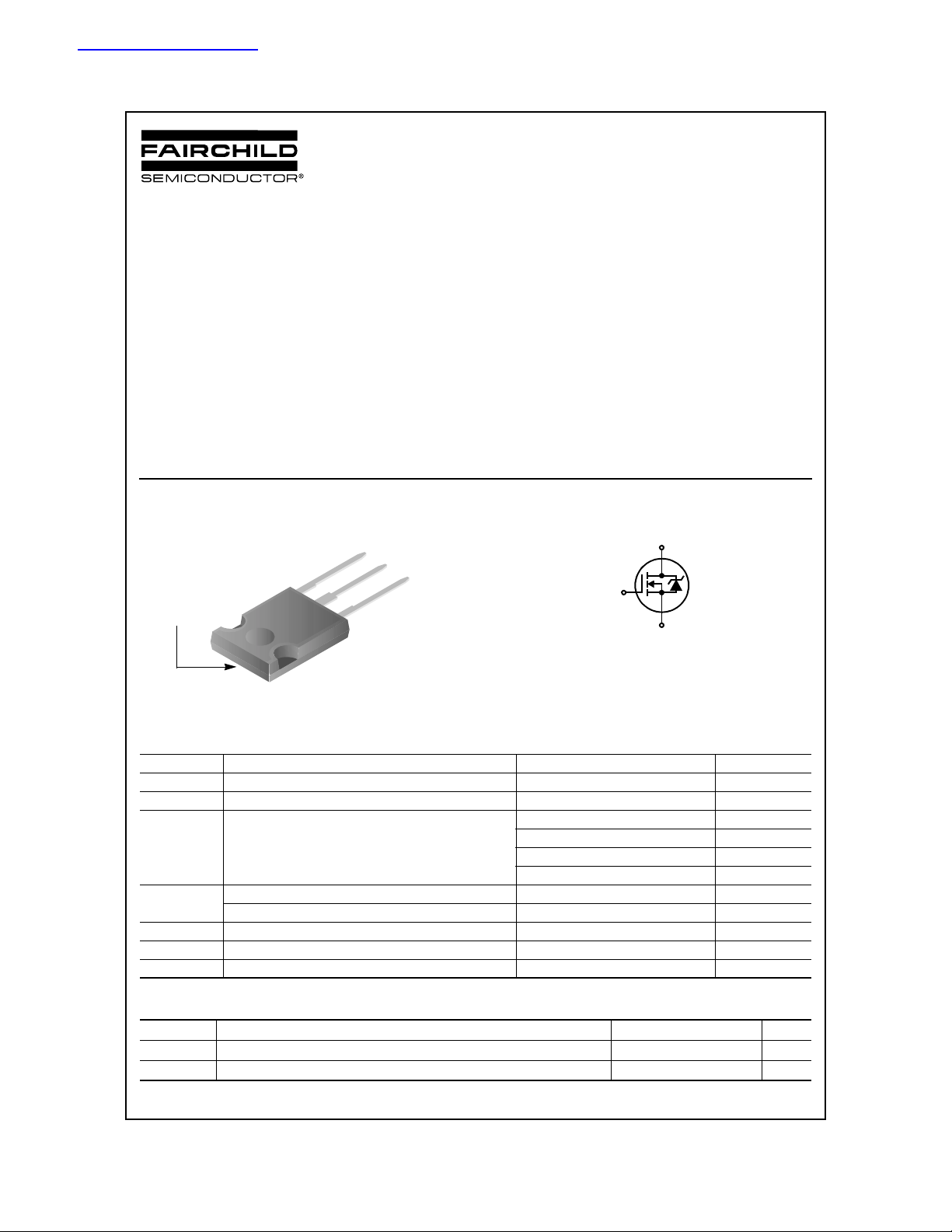
Package
JEDEC TO-247
SOURCE
DRAIN
DRAIN
(FLANGE)
GATE
Features
• Low Gate Charge Qg results in Simple Drive
Requirement
• Improved Gate, Avalanche and High Reapplied dv/dt
Ruggedness
• Reduced r
DS(ON)
• Reduced Miller Capacitance and Low Input Capacitance
• Improved Switching Speed with Low EMI
• 175°C Rated Junction Temperature
Symbol
D
G
S
Absolute Maximum Ratings T
o
= 25
C unless otherwise noted
C
Symbol Parameter Ratings Units
V
DSS
V
GS
Drain to Source Voltage 500 V
Gate to Source Voltage ±30 V
Drain Current
I
D
Continuous (T
Continuous (T
Pulsed
P
, T
T
J
Power dissipation 750 W
D
Derate above 25
Operating and Storage Temperature -55 to 175
STG
= 25oC, VGS = 10V) 44 A
C
= 100oC, VGS = 10V) 32 A
C
1
o
C5W/
176 A
Soldering Temperature for 10 seconds 300 (1.6mm from case)
Mounting Torque, 8-32 or M3 Screw 10ibf*in (1.1N*m)
Thermal Characteristics
R
R
R
©2002 Fairchild Semiconductor Corporation
Thermal Resistance Junction to Case 0.2
θJC
Thermal Resistance Case to Sink, Flat, Greased Surface 0.24
θCS
Thermal Resistance Junction to Ambient 40
θJA
o
C
o
C
o
C
o
C/W
o
C/W
o
C/W
FDH44N50 Rev. A4, August 2002

Package Marking and Ordering Information
Device Marking Device Package Reel Size Tape Width Quantity
FDH44N50 FDH44N50 TO-247 - - 30
FDH44N50
Electrical Characteristics
TJ = 25°C (unless otherwise noted)
Symbol Parameter Tes t C onditions Min Typ Max Units
Statics
∆B
B
VDSS
VDSS
r
DS(ON)
V
GS(th)
I
DSS
I
GSS
Drain to Source Breakdown Voltage ID = 250µA, VGS = 0V 500 - - V
/∆TJBreakdown Voltage Temp. Coefficient
Reference to 25
ID = 1mA
o
C,
-0.61-V/°C
Drain to Source On-Resistance VGS = 10V, ID = 22A - 0.11 0.12 Ω
Gate Threshold Voltage VDS = VGS, ID = 250µA 23.154 V
V
= 500V TC = 25oC- - 25
Zero Gate Voltage Drain Current
DS
= 0V TC = 150oC- - 250
V
GS
Gate to Source Leakage Current VGS = ±20V - - ±100 nA
Dynamics
g
Q
g(TOT)
Q
Q
t
d(ON)
t
d(OFF)
C
C
OSS
C
RSS
Forward Transconductance VDS = 50V, ID = 22A 11 - - S
fs
Total Gate Charge at 10V
Gate to Source Gate Charge - 24 29 nC
gs
Gate to Drain “Miller” Charge - 31 37 nC
gd
Tur n-On Delay Time
Rise Time - 84 - ns
t
r
Turn-Off Delay Time - 45 - ns
t
Fall Time -79-ns
f
Input Capacitance
ISS
Output Capacitance - 645 - pF
Reverse Transfer Capacitance - 40 - pF
V
= 10V,
GS
V
= 400V,
DS
= 44A
I
D
= 250V,
V
DD
= 44A,
I
D
= 2.15Ω,
R
G
R
= 5.68Ω
D
= 25V, VGS = 0V,
V
DS
f = 1MHz
- 90 108 nC
-16-ns
-5335- pF
µA
Avalanche Characteristics
E
I
AR
Single Pulse Avalanche Energy
AS
Avalanche Current - - 44 A
2
1500 - - mJ
Drain-Source Diode Characteristics
I
I
SM
V
t
Q
Notes:
1: Repetitive rating; pulse width limited by maximum junction temperature
2: Starting T
©2002 Fairchild Semiconductor Corporation FDH44N50 Rev. A4, August 2002
Continuous Source Current
S
(Body Diode)
Pulsed Source Current
1
(Body Diode)
Source to Drain Diode Voltage I
SD
Reverse Recovery Time ISD = 44A, dISD/dt = 100A/µs - 920 1100 ns
rr
Reverse Recovered Charge ISD = 44A, dISD/dt = 100A/µs -1418µC
RR
= 25°C, L = 1.61mH, IAS = 44
J
MOSFET symbol
showing the
integral reverse
p-n junction diode.
= 44A - 0.900 1.2 V
SD
D
G
S
--44A
- - 176 A
 Loading...