

FDP047AN08A0 / FDI047AN08A0 / FDH047AN08A0
N-Channel PowerTrench® MOSFET
75V, 80A, 4.7mΩ
FDP047AN08A0 / FDI047AN08A0 / FDH047AN08A0
June 2004
Features
•r
•Q
• Low Miller Charge
•Low Q
• UIS Capability (Single Pulse and Repetitive Pulse)
• Qualified to AEC Q101
Formerly developmental type 82684
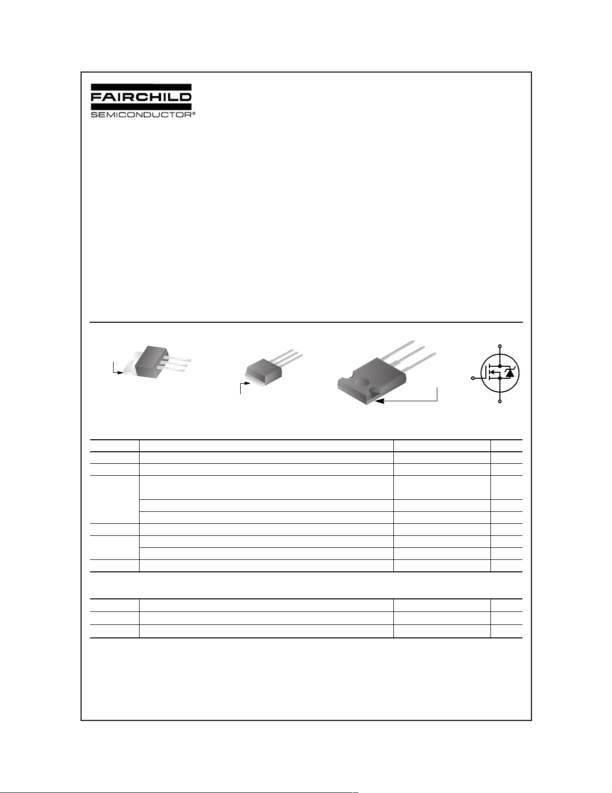
DRAIN
(FLANGE)
MOSFET Maximum Ratings T
= 4.0mΩ (Typ.), V
DS(ON)
(tot) = 92nC (Typ.), V
g
Body Diode
RR
TO-220AB
FDP SERIES
GS
GATE
GS
= 10V
SOURCE
DRAIN
= 10V, ID = 80A
DRAIN
(FLANGE)
C
SOURCE
TO-262AB
FDI SERIES
= 25°C unless otherwise noted
Applications
• 42V Automotive Load Control
• Starter / Alternator Systems
• Electronic Power Steering Systems
• Electronic Valve Train Systems
• DC-DC converters and Off-line UPS
• Distributed Power Architectures and VRMs
• Primary Switch for 24V and 48V systems
SOURCE
DRAIN
GATE
TO-24 7
FDH SERIES
DRAIN
DRAIN
(
FLANGE
GATE
G
)
Symbol Parameter Ratings Units
V
DSS
V
GS
Drain to Source Voltage 75 V
Gate to Source Voltage ±20 V
Drain Current
I
D
Continuous (T
Continuous (T
< 144oC, VGS = 10V)
C
= 25oC, VGS = 10V, with R
C
= 62oC/W) 15 A
θJA
80 A
Pulsed Figure 4 A
E
AS
P
D
, T
T
J
STG
Single Pulse Avalanche Energy (Note 1) 475 mJ
Power dissipation 310 W
o
Derate above 25
C2.0W/
Operating and Storage Temperature -55 to 175
D
S
o
C
o
C
Thermal Characteristics
R
θJC
R
θJA
R
θJA
This product has been designed to meet the extreme test conditions and environment demanded by the automotive industry. For a
All Fairchild Semiconductor products are manufactured, assembled and tested under ISO9000 and QS9000 quality systems
©2004 Fairchild Semiconductor Corporation
Thermal Resistance Junction to Case TO-220, TO-262, TO-247 0.48
Thermal Resistance Junction to Ambient TO-220, TO-262 (Note 2) 62
Thermal Resistance Junction to Ambient TO-247 (Note 2) 30
copy of the requirements, see AEC Q101 at: http://www.aecouncil.com/
certification.
FDP047AN08A0 / FDI047AN08A0 / FDH047AN08A0 Rev. C
o
C/W
o
C/W
o
C/W
Package Marking and Ordering Information
Device Marking Device Package Reel Size Tape Width Quantity
FDP047AN08A0 FDP047AN08A0 TO-220AB Tube N/A 50 units
FDI047AN08A0 FDI047AN08A0 TO-262AB Tube N/A 50 units
FDH047AN08A0 FDH047AN08A0 TO-247 Tube N/A 30 units
FDP047AN08A0 / FDI047AN08A0 / FDH047AN08A0
Electrical Characteristics T
= 25°C unless otherwise noted
C
Symbol Parameter Test Conditions Min Typ Max Units
Off Characteristics
B
I
DSS
I
GSS
VDSS
Drain to Source Breakdown Voltage ID = 250µA, VGS = 0V 75 - - V
V
= 60V - - 1
Zero Gate Voltage Drain Current
DS
= 0V TC = 150oC - - 250
V
GS
Gate to Source Leakage Current VGS = ±20V - - ±100 nA
On Characteristics
V
GS(TH)
r
DS(ON)
Gate to Source Threshold Voltage VGS = VDS, ID = 250µA2-4V
= 80A, VGS = 10V - 0.0040 0.0047
I
D
I
= 37A, VGS = 6V - 0.0058 0.0087
Drain to Source On Resistance
D
= 80A, VGS = 10V,
I
D
T
= 175oC
J
- 0.0082 0.011
Dynamic Characteristics
C
C
C
Q
Q
Q
Q
Q
ISS
OSS
RSS
g(TOT)
g(TH)
gs
gs2
gd
Input Capacitance
Output Capacitance - 1000 - pF
Reverse Transfer Capacitance - 240 - pF
= 25V, VGS = 0V,
V
DS
f = 1MHz
Total Gate Charge at 10V VGS = 0V to 10V
Threshold Gate Charge VGS = 0V to 2V - 11 17 nC
Gate to Source Gate Charge - 27 - nC
Gate Charge Threshold to Plateau - 16 - nC
V
DD
= 80A
I
D
= 1.0mA
I
g
= 40V
Gate to Drain “Miller” Charge - 21 - nC
- 6600 - pF
92 138 nC
µA
Ω
Switching Characteristics
t
ON
t
d(ON)
t
r
t
d(OFF)
t
f
t
OFF
Tur n -O n T i m e
Turn-On Delay Time - 18 - ns
Rise Time - 88 - ns
Turn-Off Delay Time - 40 - ns
Fall Time - 45 - ns
Turn-Off Time - - 128 ns
(VGS = 10V)
= 40V, ID = 80A
V
DD
= 10V, RGS = 3.3Ω
V
GS
- - 160 ns
Drain-Source Diode Characteristics
I
= 80A - - 1.25 V
V
SD
t
rr
Q
RR
Notes:
1: Starting TJ = 25°C, L = 0.232mH, IAS = 64A.
2: Pulse Width = 100s
©2004 Fairchild Semiconductor Corporation FDP047AN08A0 / FDI047AN08A0 / FDH047AN08A0 Rev. C
Source to Drain Diode Voltage
Reverse Recovery Time ISD = 75A, dISD/dt = 100A/µs- -53ns
Reverse Recovered Charge ISD = 75A, dISD/dt = 100A/µs- -54nC
SD
= 40A - - 1.0 V
I
SD
FDP047AN08A0 / FDI047AN08A0 / FDH047AN08A0
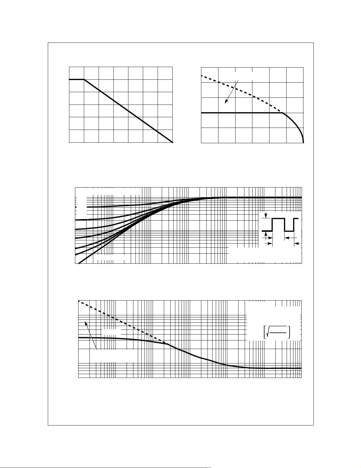
Typical Characteristics T
1.2
1.0
0.8
0.6
0.4
0.2
POWER DISSIPATION MULTIPLIER
0
0 25 50 75 100 175
TC, CASE TEMPERATURE (oC)
= 25°C unless otherwise noted
C
150
125
Figure 1. Normalized Power Dissipation vs Case
Temperature
2
DUTY CYCLE - DESCENDING ORDER
0.5
1
0.2
0.1
0.05
0.02
0.01
0.1
, NORMALIZED
θJC
Z
THERMAL IMPEDANCE
0.01
-5
10
SINGLE PULSE
-4
10
-3
10
t, RECTANGULAR PULSE DURATION (s)
200
CURRENT LIMITED
160
120
80
, DRAIN CURRENT (A)
D
I
40
0
25 50 75 100 125 150 175
BY PACKAGE
TC, CASE TEMPERATURE (oC)
Figure 2. Maximum Continuous Drain Current vs
Case Temperature
P
DM
t
1
t
x R
2
2
+ T
θJC
C
1
10
NOTES:
DUTY FACTOR: D = t1/t
PEAK TJ = PDM x Z
-2
10
-1
10
θJC
10
0
Figure 3. Normalized Maximum Transient Thermal Impedance
2000
1000
VGS = 10V
, PEAK CURRENT (A)
DM
I
100
50
10
TRANSCONDUCTANCE
MAY LIMIT CURRENT
IN THIS REGION
-5
-4
10
-3
10
-2
10
t, PULSE WIDTH (s)
-1
10
TC = 25oC
FOR TEMPERATURES
ABOVE 25oC DERATE PEAK
CURRENT AS FOLLOWS:
175 - T
I = I
25
10
C
150
0
1
10
Figure 4. Peak Current Capability
©2004 Fairchild Semiconductor Corporation FDP047AN08A0 / FDI047AN08A0 / FDH047AN08A0 Rev. C

FDP047AN08A0 / FDI047AN08A0 / FDH047AN08A0
Typical Characteristics T
2000
1000
100
10
OPERATION IN THIS
AREA MAY BE
LIMITED BY r
, DRAIN CURRENT (A)
D
I
1
SINGLE PULSE
TJ = MAX RATED
TC = 25oC
0.1
0.1 1 10 100
DS(ON)
VDS, DRAIN TO SOURCE VOLTAGE (V)
= 25°C unless otherwise noted
C
10µs
100µs
1ms
10ms
DC
Figure 5. Forward Bias Safe Operating Area
150
PULSE DURATION = 80µs
DUTY CYCLE = 0.5% MAX
V
= 15V
DD
120
90
TJ = 175oC
60
, DRAIN CURRENT (A)
I
TJ = 25oC
D
30
0
4.0 4.5 5.0 5.5 6.0
VGS, GATE TO SOURCE VOLTAGE (V)
TJ = -55oC
500
If R = 0
tAV = (L)(IAS)/(1.3*RATED BV
If R ≠ 0
tAV = (L/R)ln[(IAS*R)/(1.3*RATED BV
100
10
, AVALANCHE CURRENT (A)
AS
STARTING TJ = 150oC
I
1
.01 0.1 1 10 100
tAV, TIME IN AVALANCHE (ms)
- VDD)
DSS
- VDD) +1]
DSS
STARTING TJ = 25oC
NOTE: Refer to Fairchild Application Notes AN7514 and AN7515
Figure 6. Unclamped Inductive Switching
Capability
150
VGS = 10V
120
VGS = 6V
90
60
, DRAIN CURRENT (A)
D
I
30
0
0 0.5 1.0 1.5
VDS, DRAIN TO SOURCE VOLTAGE (V)
PULSE DURATION = 80µs
DUTY CYCLE = 0.5% MAX
VGS = 7V
VGS = 5V
TC = 25oC
Figure 7. Transfer Characteristics Figure 8. Saturation Characteristics
7
PULSE DURATION = 80µs
DUTY CYCLE = 0.5% MAX
6
VGS = 6V
5
4
DRAIN TO SOURCE ON RESISTANCE(mΩ)
3
0 20406080
VGS = 10V
I
, DRAIN CURRENT (A)
D
Figure 9. Drain to Source On Resistance vs Drain
Current
©2004 Fairchild Semiconductor Corporation FDP047AN08A0 / FDI047AN08A0 / FDH047AN08A0 Rev. C
2.5
PULSE DURATION = 80µs
DUTY CYCLE = 0.5% MAX
2.0
1.5
ON RESISTANCE
1.0
NORMALIZED DRAIN TO SOURCE
0.5
-80 -40 0 40 80 120 160 200
TJ, JUNCTION TEMPERATURE (oC)
VGS = 10V, ID = 80A
Figure 10. Normalized Drain to Source On
Resistance vs Junction Temperature

FDP047AN08A0 / FDI047AN08A0 / FDH047AN08A0
Typical Characteristics T
1.2
1.0
0.8
NORMALIZED GATE
THRESHOLD VOLTAGE
0.6
0.4
-80 -40 0 40 80 120 160 200
TJ, JUNCTION TEMPERATURE (oC)
= 25°C unless otherwise noted
C
VGS = VDS, ID = 250µA
Figure 11. Normalized Gate Threshold Voltage vs
Junction Temperature
10000
C
= CGS + C
ISS
C
≅ C
+ C
OSS
DS
GD
1000
C
= C
RSS
GD
C, CAPACITANCE (pF)
V
= 0V, f = 1MHz
GS
100
0.1 1 10 75
VDS, DRAIN TO SOURCE VOLTAGE (V)
GD
1.15
ID = 250µA
1.10
1.05
1.00
BREAKDOWN VOLTAGE
0.95
NORMALIZED DRAIN TO SOURCE
0.90
-80 -40 0 40 80 120 160 200
TJ, JUNCTION TEMPERATURE (oC)
Figure 12. Normalized Drain to Source
Breakdown Voltage vs Junction Temperature
10
VDD = 40V
8
6
4
WAVEFOR MS IN
2
, GATE TO SOURCE VOLTAGE (V)
GS
V
0
0 25 50 75 100
Qg, GATE CHARGE (nC)
DESCENDING ORDER:
ID = 80A
ID = 10A
Figure 13. Capacitance vs Drain to Source
Voltage
©2004 Fairchild Semiconductor Corporation FDP047AN08A0 / FDI047AN08A0 / FDH047AN08A0 Rev. C
Figure 14. Gate Charge Waveforms for Constant
Gate Currents

Test Circuits and Waveforms
V
DS
L
VAR Y tP TO OBTAIN
REQUIRED PEAK I
V
GS
R
AS
G
+
V
DD
-
I
AS
DUT
t
0V
P
I
AS
0.01Ω
0
Figure 15. Unclamped Energy Test Circuit Figure 16. Unclamped Energy Waveforms
V
DS
V
DD
V
Q
I
g(REF)
L
V
GS
DUT
+
V
DD
-
V
0
I
g(REF)
GS
= 2V
Q
gs2
Q
g(TH)
Q
gs
0
Figure 17. Gate Charge Test Circuit Figure 18. Gate Charge Waveforms
BV
DSS
t
P
t
AV
Q
g(TOT)
DS
gd
V
GS
FDP047AN08A0 / FDI047AN08A0 / FDH047AN08A0
V
DS
V
DD
V
= 10V
GS
V
DS
R
L
V
GS
R
GS
V
GS
DUT
+
V
DD
-
V
DS
0
V
GS
10%
0
t
d(ON)
90%
t
ON
50%
10%
t
r
PULSE WIDTH
t
d(OFF)
90%
t
OFF
50%
t
f
90%
10%
Figure 19. Switching Time Test Circuit Figure 20. Switching Time Waveforms
©2004 Fairchild Semiconductor Corporation FDP047AN08A0 / FDI047AN08A0 / FDH047AN08A0 Rev. C

PSPICE Electrical Model
.SUBCKT FDP047AN08A0 2 1 3 ; rev March 2002
CA 12 8 1.5e-9
CB 15 14 1.5e-9
CIN 6 8 6.4e-9
DBODY 7 5 DBODYMOD
DBREAK 5 11 DBREAKMOD
DPLCAP 10 5 DPLCAPMOD
EBREAK 11 7 17 18 82.3
EDS 14 8 5 8 1
EGS 13 8 6 8 1
ESG 6 10 6 8 1
EVTHRES 6 21 19 8 1
EVTEMP 20 6 18 22 1
IT 8 17 1
LDRAIN 2 5 1e-9
LGATE 1 9 4.81e-9
LSOURCE 3 7 4.63e-9
MMED 16 6 8 8 MMEDMOD
MSTRO 16 6 8 8 MSTROMOD
MWEAK 16 21 8 8 MWEAKMOD
RBREAK 17 18 RBREAKMOD 1
RDRAIN 50 16 RDRAINMOD 9e-4
RGATE 9 20 1.36
RLDRAIN 2 5 10
RLGATE 1 9 48.1
RLSOURCE 3 7 46.3
RSLC1 5 51 RSLCMOD 1e-6
RSLC2 5 50 1e3
RSOURCE 8 7 RSOURCEMOD 2.3e-3
RVTHRES 22 8 RVTHRESMOD 1
RVTEMP 18 19 RVTEMPMOD 1
GATE
1
LGATE
RLGATE
RGATE
9
12
CA
-
ESG
+
EVTEMP
+
-
18
22
20
S1A
13814
S1B
13
EGS EDS
10
6
8
+
+
RSLC2
6
S2A
13
S2B
6
8
-
-
DPLCAP
EVTHRES
+
19
8
CIN
15
CB
-
+
-
5
51
5
51
MSTRO
14
5
8
RSLC1
+
ESLC
50
RDRAIN
16
21
8
MMED
DBREAK
EBREAK
MWEAK
RSOURCE
RBREAK
17 18
IT
8
RVTHRES
FDP047AN08A0 / FDI047AN08A0 / FDH047AN08A0
LDRAIN
RLDRAIN
11
+
17
DBODY
18
-
LSOURCE
7
RLSOURCE
RVTE MP
19
VBAT
+
22
DRAIN
2
SOURCE
3
S1A 6 12 13 8 S1AMOD
S1B 13 12 13 8 S1BMOD
S2A 6 15 14 13 S2AMOD
S2B 13 15 14 13 S2BMOD
VBAT 22 19 DC 1
ESLC 51 50 VALUE={(V(5,51)/ABS(V(5,51)))*(PWR(V(5,51)/(1e-6*250),10))}
.MODEL DBODYMOD D (IS = 2.4e-11 N = 1.04 RS = 1.76e-3 TRS1 = 2.7e-3 TRS2 = 2e-7 XTI=3.9 CJO = 4.35e-9 TT = 1e-8
M = 5.4e-1)
.MODEL DBREAKMOD D (RS = 1.5e-1 TRS1 = 1e-3 TRS2 = -8.9e-6)
.MODEL DPLCAPMOD D (CJO = 1.35e-9 IS = 1e-30 N = 10 M = 0.53)
.MODEL MMEDMOD NMOS (VTO = 3.7 KP = 9 IS =1e-30 N = 10 TOX = 1 L = 1u W = 1u RG = 1.36)
.MODEL MSTROMOD NMOS (VTO = 4.4 KP = 250 IS = 1e-30 N = 10 TOX = 1 L = 1u W = 1u)
.MODEL MWEAKMOD NMOS (VTO = 3.05 KP = 0.03 IS = 1e-30 N = 10 TOX = 1 L = 1u W = 1u RG = 1.36e1 RS = 0.1)
.MODEL RBREAKMOD RES (TC1 = 1.05e-3 TC2 = -9e-7)
.MODEL RDRAINMOD RES (TC1 = 1.9e-2 TC2 = 4e-5)
.MODEL RSLCMOD RES (TC1 = 1.3e-3 TC2 = 1e-5)
.MODEL RSOURCEMOD RES (TC1 = 1e-3 TC2 = 1e-6)
.MODEL RVTHRESMOD RES (TC1 = -6e-3 TC2 = -1.9e-5)
.MODEL RVTEMPMOD RES (TC1 = -2.4e-3 TC2 = 1e-6)
.MODEL S1AMOD VSWITCH (RON = 1e-5 ROFF = 0.1 VON = -4.0 VOFF= -1.5)
.MODEL S1BMOD VSWITCH (RON = 1e-5 ROFF = 0.1 VON = -1.5 VOFF= -4.0)
.MODEL S2AMOD VSWITCH (RON = 1e-5 ROFF = 0.1 VON = -1.0 VOFF= 0.5)
.MODEL S2BMOD VSWITCH (RON = 1e-5 ROFF = 0.1 VON = 0.5 VOFF= -1.0)
.ENDS
Note: For further discussion of the PSPICE model, consult A New PSPICE Sub-Circuit for the Power MOSFET Featuring Global
Temperature Options; IEEE Power Electronics Specialist Conference Records, 1991, written by William J. Hepp and C. Frank
Wheatley.
©2004 Fairchild Semiconductor Corporation FDP047AN08A0 / FDI047AN08A0 / FDH047AN08A0 Rev. C

SABER Electrical Model
REV March 2002
template FDP047AN08A0 n2,n1,n3
electrical n2,n1,n3
{
var i iscl
dp..model dbodymod = (isl = 2.4e-11, n1 = 1.04, rs = 1.76e-3, trs1 = 2.7e-3, trs2 = 2e-7, xti = 3.9, cjo = 4.35e-9, tt = 1e-8, m = 5.4e-1)
dp..model dbreakmod = (rs = 1.5e-1, trs1 = 1e-3, trs2 = -8.9e-6)
dp..model dplcapmod = (cjo = 1.35e-9, isl =10e-30, nl =10, m = 0.53)
m..model mmedmod = (type=_n, vto = 3.7, kp = 9, is =1e-30, tox=1)
m..model mstrongmod = (type=_n, vto = 4.4, kp = 250, is = 1e-30, tox = 1)
m..model mweakmod = (type=_n, vto = 3.05, kp = 0.03, is = 1e-30, tox = 1, rs=0.1)
sw_vcsp..model s1amod = (ron = 1e-5, roff = 0.1, von = -4.0, voff = -1.5)
sw_vcsp..model s1bmod = (ron =1e-5, roff = 0.1, von = -1.5, voff = -4.0)
sw_vcsp..model s2amod = (ron = 1e-5, roff = 0.1, von = -1.0, voff = 0.5)
sw_vcsp..model s2bmod = (ron = 1e-5, roff = 0.1, von = 0.5, voff = -1.0)
c.ca n12 n8 = 1.5e-9
10
c.cb n15 n14 = 1.5e-9
c.cin n6 n8 = 6.4e-9
RSLC2
dp.dbody n7 n5 = model=dbodymod
dp.dbreak n5 n11 = model=dbreakmod
dp.dplcap n10 n5 = model=dplcapmod
i.it n8 n17 = 1
l.ldrain n2 n5 = 1e-9
l.lgate n1 n9 = 4.81e-9
GATE
l.lsource n3 n7 = 4.63e-9
LGATE
1
RLGATE
RGATE
9
ESG
EVTEMP
+
18
22
20
6
8
+
6
-
m.mmed n16 n6 n8 n8 = model=mmedmod, l=1u, w=1u
m.mstrong n16 n6 n8 n8 = model=mstrongmod, l=1u, w=1u
m.mweak n16 n21 n8 n8 = model=mweakmod, l=1u, w=1u
res.rbreak n17 n18 = 1, tc1 = 1.05e-3, tc2 = -9e-7
res.rdrain n50 n16 = 9e-4, tc1 = 1.9e-2, tc2 = 4e-5
res.rgate n9 n20 = 1.36
res.rldrain n2 n5 = 10
res.rlgate n1 n9 = 48.1
res.rlsource n3 n7 = 46.3
res.rslc1 n5 n51= 1e-6, tc1 = 1e-3, tc2 =1e-5
res.rslc2 n5 n50 = 1e3
res.rsource n8 n7 = 2.3e-3, tc1 = 1e-3, tc2 =1e-6
12
CA
S1A
13814
13
S1B
13
+
+
6
EGS EDS
8
-
-
res.rvtemp n18 n19 = 1, tc1 = -2.4e-3, tc2 = 1e-6
res.rvthres n22 n8 = 1, tc1 = -6e-3, tc2 = -1.9e-5
DPLCAP
EVTHRES
+
19
8
S2A
S2B
5
RSLC1
51
ISCL
8
MMED
8
DBREAK
11
MWEAK
EBREAK
+
RSOURCE
RBREAK
17 18
IT
RVTHR ES
50
RDRAIN
16
21
-
MSTRO
CIN
15
CB
14
+
5
8
-
17
18
7
RVT EMP
19
-
+
22
LDRAIN
RLDRAIN
DBODY
LSOURCE
RLSOURCE
VBAT
DRAIN
2
SOURCE
3
FDP047AN08A0 / FDI047AN08A0 / FDH047AN08A0
spe.ebreak n11 n7 n17 n18 = 82.3
spe.eds n14 n8 n5 n8 = 1
spe.egs n13 n8 n6 n8 = 1
spe.esg n6 n10 n6 n8 = 1
spe.evtemp n20 n6 n18 n22 = 1
spe.evthres n6 n21 n19 n8 = 1
sw_vcsp.s1a n6 n12 n13 n8 = model=s1amod
sw_vcsp.s1b n13 n12 n13 n8 = model=s1bmod
sw_vcsp.s2a n6 n15 n14 n13 = model=s2amod
sw_vcsp.s2b n13 n15 n14 n13 = model=s2bmod
v.vbat n22 n19 = dc=1
equations {
i (n51->n50) +=iscl
iscl: v(n51,n50) = ((v(n5,n51)/(1e-9+abs(v(n5,n51))))*((abs(v(n5,n51)*1e6/250))** 10))
}
}
©2004 Fairchild Semiconductor Corporation FDP047AN08A0 / FDI047AN08A0 / FDH047AN08A0 Rev. C
FDP047AN08A0 / FDI047AN08A0 / FDH047AN08A0
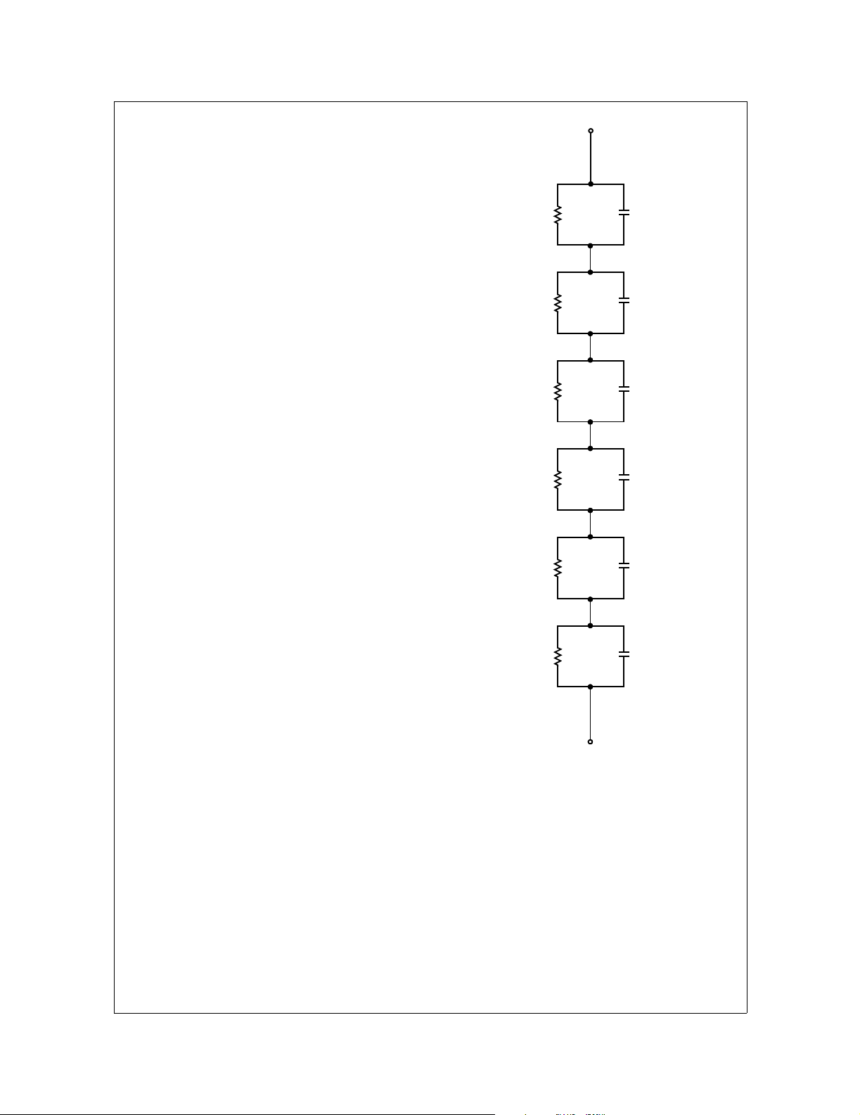
SPICE Thermal Model
REV 23 March 2002
FDP047AN08A0T
CTHERM1 th 6 6.45e-3
CTHERM2 6 5 3e-2
CTHERM3 5 4 1.4e-2
CTHERM4 4 3 1.65e-2
CTHERM5 3 2 4.85e-2
CTHERM6 2 tl 1e-1
RTHERM1 th 6 3.24e-3
RTHERM2 6 5 8.08e-3
RTHERM3 5 4 2.28e-2
RTHERM4 4 3 1e-1
RTHERM5 3 2 1.1e-1
RTHERM6 2 tl 1.4e-1
SABER Thermal Model
SABER thermal model FDP047AN08A0T
template thermal_model th tl
thermal_c th, tl
{
ctherm.ctherm1 th 6 = 6.45e-3
ctherm.ctherm2 6 5 = 3e-2
ctherm.ctherm3 5 4 = 1.4e-2
ctherm.ctherm4 4 3 = 1.65e-2
ctherm.ctherm5 3 2 = 4.85e-2
ctherm.ctherm6 2 tl = 1e-1
rtherm.rtherm1 th 6 = 3.24e-3
rtherm.rtherm2 6 5 = 8.08e-3
rtherm.rtherm3 5 4 = 2.28e-2
rtherm.rtherm4 4 3 = 1e-1
rtherm.rtherm5 3 2 = 1.1e-1
rtherm.rtherm6 2 tl = 1.4e-1
}
RTHERM1
RTHERM2
RTHERM3
RTHERM4
RTHERM5
JUNCTION
th
CTHERM1
6
CTHERM2
5
CTHERM3
4
CTHERM4
3
CTHERM5
RTHERM6
2
CTHERM6
tl
CASE
©2004 Fairchild Semiconductor Corporation FDP047AN08A0 / FDI047AN08A0 / FDH047AN08A0 Rev. C

TRADEMARKS
The following are registered and unregistered trademarks Fairchild Semiconductor owns or is authorized to use and is not
intended to be an exhaustive list of all such trademarks.
ACEx™
ActiveArray™
Bottomless™
CoolFET™
CROSSVOLT™
DOME™
EcoSPARK™
2
CMOS™
E
EnSigna™
FACT™
Across the board. Around the world.™
The Power Franchise
FACT Quiet Series™
®
FAST
FASTr™
FPS™
FRFET™
GlobalOptoisolator™
GTO™
HiSeC™
2
C™
I
i-Lo™
®
Programmable Active Droop™
ImpliedDisconnect™
ISOPLANAR™
LittleFET™
MICROCOUPLER™
MicroFET™
MicroPak™
MICROWIRE™
MSX™
MSXPro™
OCX™
OCXPro™
OPTOLOGIC
®
OPTOPLANAR™
PACMAN™
POP™
Power247™
PowerSaver™
PowerTrench
QFET
®
®
QS™
QT Optoelectronics™
Quiet Series™
RapidConfigure™
RapidConnect™
µSerDes™
SILENT SWITCHER
SMART START™
SPM™
Stealth™
SuperFET™
SuperSOT™-3
SuperSOT™-6
SuperSOT™-8
SyncFET™
TinyLogic
TINYOPTO™
TruTranslation™
UHC™
UltraFET
®
VCX™
®
®
DISCLAIMER
FAIRCHILD SEMICONDUCTOR RESERVES THE RIGHT TO MAKE CHANGES WITHOUT FURTHER NOTICE TO ANY
PRODUCTS HEREIN TO IMPROVE RELIABILITY, FUNCTION OR DESIGN. FAIRCHILD DOES NOT ASSUME ANY
LIABILITY ARISING OUT OF THE APPLICATION OR USE OF ANY PRODUCT OR CIRCUIT DESCRIBED HEREIN;
NEITHER DOES IT CONVEY ANY LICENSE UNDER ITS PATENT RIGHTS, NOR THE RIGHTS OF OTHERS.
LIFE SUPPORT POLICY
FAIRCHILD’S PRODUCTS ARE NOT AUTHORIZED FOR USE AS CRITICAL COMPONENTS IN LIFE SUPPORT
DEVICES OR SYSTEMS WITHOUT THE EXPRESS WRITTEN APPROVAL OF FAIRCHILD SEMICONDUCTOR
CORPORATION.
As used herein:
1. Life support devices or systems are devices or systems
which, (a) are intended for surgical implant into the body,
or (b) support or sustain life, or (c) whose failure to perform
when properly used in accordance with instructions for use
provided in the labeling, can be reasonably expected to
result in significant injury to the user.
2. A critical component is any component of a life support
device or system whose failure to perform can be
reasonably expected to cause the failure of the life support
device or system, or to affect its safety or effectiveness.
PRODUCT STATUS DEFINITIONS
Definition of Terms
Datasheet Identification Product Status Definition
Advance Information Formative or In
Design
Preliminary First Production This datasheet contains preliminary data, and
No Identification Needed Full Production This datasheet contains final specifications. Fairchild
Obsolete Not In Production This datasheet contains specifications on a product
This datasheet contains the design specifications for
product development. Specifications may change in
any manner without notice.
supplementary data will be published at a later date.
Fairchild Semiconductor reserves the right to make
changes at any time without notice in order to improve
design.
Semiconductor reserves the right to make changes at
any time without notice in order to improve design.
that has been discontinued by Fairchild semiconductor.
The datasheet is printed for reference information only.
Rev. I11
 Loading...