

Page 1
tm
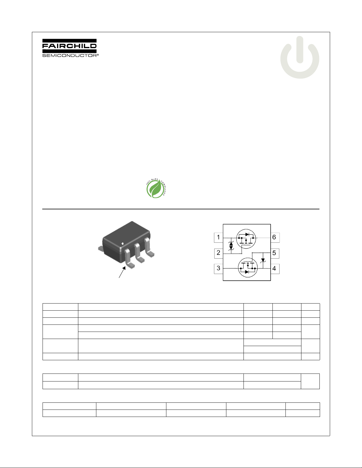
FDG8842CZ
Complementary PowerTrench® MOSFET
Q1:30V,0.75A,0.4Ω; Q2:–25V,–0.41A,1.1Ω
FDG8842CZ Complementary PowerTrench
April 2007
Features
Q1: N-Channel
Max r
Max r
Q2: P-Channel
Max r
Max r
Very low level gate drive requirements allowing direct
operation in 3V circuits(V
Very small package outline SC70-6
RoHS Compliant
= 0.4Ω at VGS = 4.5V, ID = 0.75A
DS(on)
= 0.5Ω at VGS = 2.7V, ID = 0.67A
DS(on)
= 1.1Ω at VGS = –4.5V, ID = –0.41A
DS(on)
= 1.5Ω at VGS = –2.7V, ID = –0.25A
DS(on)
<1.5V)
GS(th)
S2
G2
D1
SC70-6
Pin 1
D2
G1
S1
General Description
These N & P-Channel logic level enhancement mode field effect
transistors are produced using Fairchild’s proprietary, high cell
density, DMOS technology. This very high density process is
especially tailored to minimize on-state resistance. This
device has been designed especially for low voltage applica
tions as a replacement for bipolar digital transistors and small
signal MOSFETs. Since bias resistors are not required, this dual
digital FET can replace several different digital transistors, with
different bias resistor values.
S1
G1
D2
Q1
Q2
D1
G2
S2
-
®
MOSFET
MOSFET Maximum Ratings T
Symbol Parameter Q1 Q2 Units
V
DS
V
GS
I
D
P
D
, T
T
J
STG
Thermal Characteristics
R
θJA
R
θJA
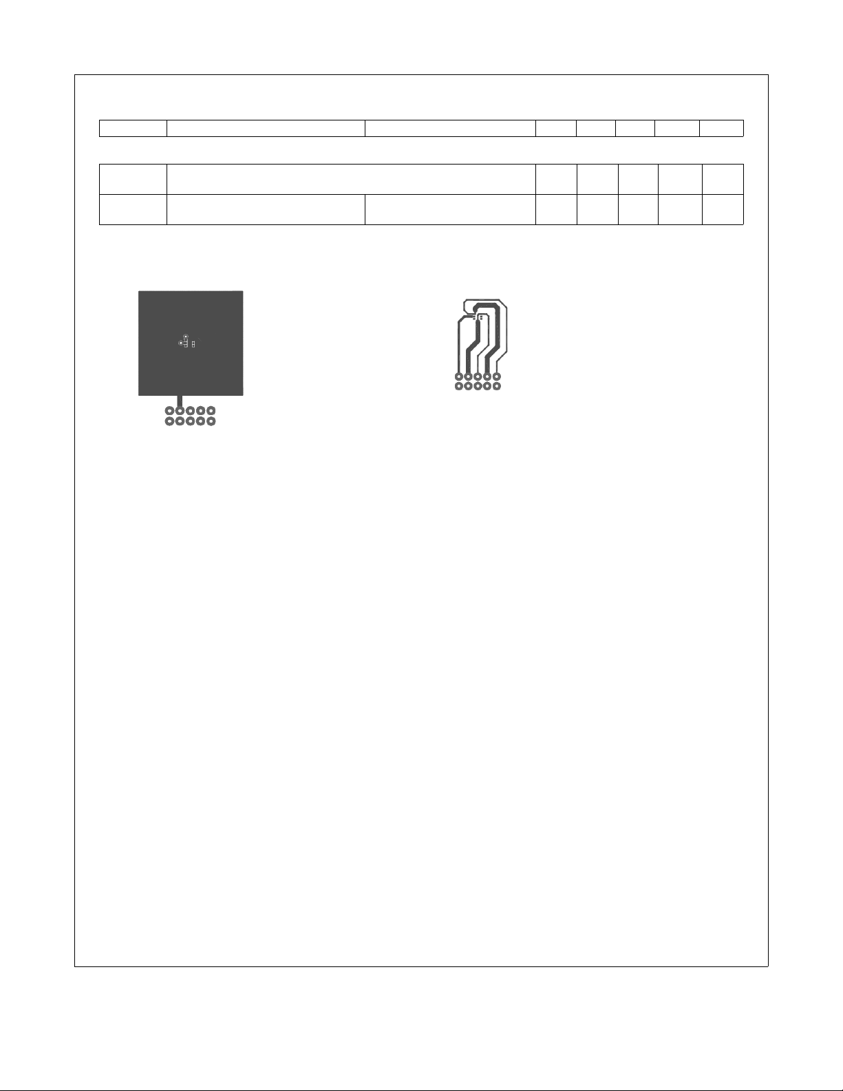
Package Marking and Ordering Information
Device Marking Device Reel Size Tape Width Quantity
©2007 Fairchild Semiconductor Corporation
FDG8842CZ Rev.B
Drain to Source Voltage 30 –25 V
Gate to Source Voltage ±12 –8 V
Drain Current -Continuous 0.75 –0.41
-Pulsed 2.2 –1.2
Power Dissipation for Single Operation (Note 1a)
(Note 1b)
Operating and Storage Junction Temperature Range –55 to +150 °C
Thermal Resistance, Junction to Ambient Single operation (Note 1a) 350
Thermal Resistance, Junction to Ambient Single operation (Note 1b) 415
.42 FDG8842CZ 7” 8mm 3000 units
= 25°C unless otherwise noted
A
1
0.36
0.30
A
W
°C/W
www.fairchildsemi.com
Page 2
FDG8842CZ Complementary PowerTrench
Electrical Characteristics T
= 25°C unless otherwise noted
J
Symbol Parameter Test Conditions Typ e Min Typ Max Units
Off Characteristics
BV
ΔBV
ΔT
I
DSS
I
GSS
DSS
DSS
J
Drain to Source Breakdown
Voltage
Breakdown Voltage Temperature
Coefficient
Zero Gate Voltage Drain Current
Gate to Source Leakage Current
On Characteristics
V
GS(th)
ΔV
ΔT
r
DS(on)
g
FS
GS(th)
J
Gate to Source Threshold Voltage
Gate to Source Threshold Voltage
Temperature Coefficient
Static Drain to Source On
Resistance
Forward Transconductance
ID = 250μA, VGS = 0V
ID = –250μA, VGS = 0V
ID = 250μA, referenced to 25°C
ID = –250μA, referenced to 25°C
VDS = 24V, V
VDS = –20V, V
GS
GS
= 0V
= 0V
VGS = ±12V, VDS= 0V
VGS = –8V, VDS= 0V
VGS = VDS, ID = 250μA
VGS = VDS, ID = –250μA
ID = 250μA, referenced to 25°C
ID = –250μA, referenced to 25°C
VGS = 4.5V, ID = 0.75A
VGS = 2.7V, ID = 0.67A
VGS = 4.5V, ID = 0.75A ,TJ = 125°C
VGS = –4.5V, ID = –0.41A
VGS = –2.7V, ID = –0.25A
VGS = –4.5V, ID = –0.41A ,TJ = 125°C
VDS = 5V, ID = 0.75A
VDS = –5V, ID = –0.41A
Q1Q2 30
–25
Q1
Q2
Q1
Q2
Q1
Q2
Q1Q20.65
–0.65
Q1
Q2
Q1
Q2
Q1
Q2
V
25
–21
1.0
–0.8
–3.0
1.8
0.25
0.29
0.36
0.87
1.20
1.22
3
8
mV/°C
1
–1
±10
–100μAnA
1.5
–1.5
mV/°C
0.4
0.5
0.6
1.1
1.5
1.9
μA
Ω
S
V
®
MOSFET
Dynamic Characteristics
C
iss
C
oss
C
rss
Input Capacitance
Output Capacitance
Reverse Transfer Capacitance
Switching Characteristics
t
d(on)
t
r
t
d(off)
t
f
Q
Q
Q
g
gs
gd
Turn-On Delay Time
Rise Time
Turn-Off Delay Time
Fall Time
Total Gate Charge
Gate to Source Charge
Gate to Drain “Miller” Charge
(note 2)
Q1
V
= 10V, VGS = 0V, f= 1MHZ
DS
Q2
V
= –10V, VGS = 0V, f= 1MHZ
DS
Q1
VDD = 5V, ID = 0.5A,
VGS = 4.5V,R
Q2
GEN
= 6Ω
VDD = –5V, ID = –0.5A,
VGS = –4.5V,R
GEN
= 6Ω
Q1
V
=4.5V, VDD = 5V, ID = 0.75A
GS
Q2
V
= –4.5V, VDD = –5V, ID = –0.41A
GS
Q1
Q2
Q1
Q2
Q1
Q2
Q1
Q2
Q1
Q2
Q1
Q2
Q1
Q2
Q1
Q2
Q1
Q2
Q1
Q2
90
70
20
30
15
15
120
100
30
40
25
25
4
10
6
12
1
10
29
9
18
56
1
10
64
1.44
1.68
pF
pF
pF
ns
ns
ns
ns
nC
nC
nC
16
35
40
1.03
1.20
0.29
0.31
0.17
0.22
©2007 Fairchild Semiconductor Corporation
FDG8842CZ Rev.B
2
www.fairchildsemi.com
Page 3
FDG8842CZ Complementary PowerTrench
Electrical Characteristics T
= 25°C unless otherwise noted
J
Symbol Parameter Test Conditions Type Min Typ Max Units
Drain-Source Diode Characteristics and Maximum Ratings
I
S
V
SD
Notes:
1. R
θJA
R
θJC
2. Pulse Test: Pulse Width < 300μs, Duty cycle < 2.0%.
Maximum Continuous Drain-Source Diode Forward Current
V
= 0V, IS = 0.3A (Note 2)
Source to Drain Diode Forward Voltage
is the sum of the junction-to-case and case-to-ambient thermal resistance where the case thermal reference is defined as the solder mounting surface of the drain pins.
is guaranteed by design while R
Scale 1:1 on letter size paper.
is determined by the user's board design.
θJA
a. 350°C/W when mounted on a
1 in2 pad of 2 oz copper .
GS
V
= 0V, IS = –0.3A (Note 2) Q1Q2
GS
Q1
Q2
0.76
–0.84
b. 415°C/W when mounted on a minimum pad
of 2 oz copper.
0.3
–0.3
1.2
–1.2
A
V
®
MOSFET
©2007 Fairchild Semiconductor Corporation
FDG8842CZ Rev.B
3
www.fairchildsemi.com
Page 4

FDG8842CZ Complementary PowerTrench
Typical Characteristics (Q1 N-Channel)T
2.20
VGS = 4.5V
1.76
1.32
0.88
, DRAIN CURRENT (A)
0.44
D
I
0.00
0.0 0.5 1.0 1.5 2.0
V
DS
Figure 1.
1.6
ID = 0.75A
V
= 4.5V
GS
1.4
1.2
1.0
NORMALIZED
0.8
DRAIN TO SOURCE ON-RESISTANCE
0.6
-50 -25 0 25 50 75 100 125 150
TJ, JUNCTION TEMPERATURE (oC)
F i g u r e 3 . N o r m a l i z e d O n - R e s i s t a n c e
vs Junction Temperature
VGS = 2.7V
PULSE DURATION = 80μs
DUTY CYCLE = 0.5%MAX
, DRAIN TO SOURCE VOLTAGE (V)
VGS = 2.0V
VGS =1.8V
VGS = 1.5V
On-Region Characteristics Figure 2.
= 25°C unless otherwise noted
J
2.6
VGS = 1.8V
2.2
1.8
1.4
NORMALIZED
1.0
PULSE DURATION = 80μs
DUTY CYCLE = 0.5%MAX
DRAIN TO SOURCE ON-RESISTANCE
0.6
0.00 0.44 0.88 1.32 1.76 2.20
I
N o r m a l i z e d O n - R e s i s t a n c e
vs Drain Current and Gate Voltage
0.8
ID =0.38A
(Ω)
0.6
, DRAIN TO
0.4
DS(on)
r
SOURCE ON-RESISTANCE
0.2
12345
Figure 4.
o
T
= 25
C
J
VGS, GATE TO SOURCE VOLTAGE (V)
O n - R es i s t a n c e vs G a t e t o
Source Voltage
VGS = 2.0V
V
GS
, DRAIN CURRENT(A)
D
PULSE DURATION = 80μs
DUTY CYCLE = 0.5%MAX
TJ = 125oC
= 2.7V
V
= 3.5V
GS
V
= 4.5V
GS
®
MOSFET
2.20
PULSE DURATION = 80μs
DUTY CYCLE = 0.5%MAX
1.76
VDD = 5V
1.32
0.88
0.44
, DRAIN CURRENT (A)
D
I
0.00
0.0 0.5 1.0 1.5 2.0 2.5
VGS, GATE TO SOURCE VOLTAGE (V)
Figure 5. Transfer Characteristics
©2007 Fairchild Semiconductor Corporation
FDG8842CZ Rev.B
TJ = 150oC
TJ = 25oC
TJ = -55oC
2
V
= 0V
GS
1
TJ = 150oC
0.1
TJ = 25oC
0.01
, REVERSE DRAIN CURRENT (A)
S
I
0.001
0.2 0.4 0.6 0.8 1.0 1.2
VSD, BODY DIODE FORWARD VOLTAGE (V)
Figure 6.
S o u r ce t o D r a i n Di o d e
TJ = -55oC
Forward Voltage vs Source Current
4
www.fairchildsemi.com
Page 5

FDG8842CZ Complementary PowerTrench
Typical Characteristics (Q1 N-Channel)T
5
ID = 0.22A
4
3
2
VDD = 5V
1
, GATE TO SOURCE VOLTAGE(V)
0
GS
V
0.00.20.40.60.81.01.21.4
Figure 7.
Qg, GATE CHARGE(nC)
Gate Charge Characteristics Figure 8.
4
1
S
r
D
0.1
SINGLE PULSE
, DRAIN CURRENT (A)
T
D
I
0.01
0.005
J
R
θJA
T
A
0.1 1 10 100
Figure 9.
D
E
T
I
M
I
L
)
n
o
(
= MAX RATED
O
= 415
C/W
O
= 25
C
VDS, DRAIN to SOURCE VOLTAGE (V)
F o r w ar d B i a s S a fe
Operating Area
VDD = 10V
V
= 15V
DD
100μs
1ms
10ms
100ms
1s
DC
= 25°C unless otherwise noted
J
200
100
10
CAPACITANCE (pF)
f = 1MHz
= 0V
V
GS
1
0.1 1 10
VDS, DRAIN TO SOURCE VOLTAGE (V)
to Source Voltage
50
10
1
, PEAK TRANSIENT POWER (W)
(PK)
P
0.1
0.0001 0.001 0.01 0.1 1 10 100 1000
Figure 10.
Single Pulse Maximum Power
C
iss
C
oss
C
rss
30
C a p a c i t a n c e v s D r a i n
SINGLE PULSE
O
R
= 415
C/W
θJA
TA = 25OC
t, PULSE WIDTH (s)
Dissipation
®
MOSFET
1
DUTY CYCLE-DESCENDING ORDER
D = 0.5
0.2
0.1
θJA
0.05
0.02
0.1
0.01
IMPEDANCE, Z
NORMALIZED THERMAL
0.01
SINGLE PULSE
0.0001 0.001 0.01 0.1 1 10 100 1000
©2007 Fairchild Semiconductor Corporation
FDG8842CZ Rev.B
NOTES:
DUTY FACTOR: D = t1/t
PEAK TJ = PDM x Z
R
= 415oC/W
θJA
t, RECTANGULAR PULSE DURATION (s)
Figure 11. Transient Thermal Response Curve
5
P
DM
x R
θJA
t
1
t
2
2
+ T
θJA
A
www.fairchildsemi.com
Page 6

FDG8842CZ Complementary PowerTrench
Typical Characteristics (Q2 P-Channel)
1.2
VGS = -4.5V
0.9
0.6
, DRAIN CURRENT (A)
D
0.3
-I
0.0
01234
Figure 13. On Region Characteristics
1.6
ID = -0.41A
V
= -4.5V
GS
1.4
1.2
1.0
NORMALIZED
0.8
DRAIN TO SOURCE ON-RESISTANCE
0.6
-50 -25 0 25 50 75 100 125 150
Figure 15. Normalized On Resistance
vs Junction Temperature
VGS = -3.5V
VGS = -2.7V
VGS = -2.5V
VGS = -2.0V
PULSE DURATION = 80μs
DUTY CYCLE = 0.5%MAX
VGS = -1.5V
-VDS, DRAIN TO SOURCE VOLTAGE (V)
TJ, JUNCTION TEMPERATURE (oC)
TJ = 25°C unless otherwise noted
5
VGS = -1.5V
4
VGS = -2.0V
3
2
NORMALIZED
1
DRAIN TO SOURCE ON-RESISTANCE
0
0.0 0.3 0.6 0.9 1.2
Figure 14. Normalized on-Resistance vs Drain
Current and Gate Voltage
4
(Ω)
3
2
, DRAIN TO
DS(on)
r
1
SOURCE ON-RESISTANCE
0
1.5 2.0 2.5 3.0 3.5 4.0 4.5 5.0
ID =-0.22A
-VGS, GATE TO SOURCE VOLTAGE (V)
Figure 16. On-Resistance vs Gate to
Source Voltage
PULSE DURATION = 80μs
DUTY CYCLE = 0.5%MAX
VGS = -2.5V
-ID, DRAIN CURRENT(A)
PULSE DURATION = 80μs
DUTY CYCLE = 0.5%MAX
VGS = -2.7V
VGS = -3.5V
VGS = -4.5V
TJ = 125oC
o
T
= 25
J
®
MOSFET
C
0.6
PULSE DURATION = 80μs
DUTY CYCLE = 0.5%MAX
VDS = -5V
0.4
0.2
, DRAIN CURRENT (A)
D
-I
0.0
0.5 1.0 1.5 2.0 2.5
-VGS, GATE TO SOURCE VOLTAGE (V)
Figure 17. Transfer Characteristics
©2007 Fairchild Semiconductor Corporation
FDG8842CZ Rev.B
TJ = -55oC
TJ = 150oC
TJ = 25oC
3
V
= 0V
GS
1
TJ = 150oC
0.1
TJ = 25oC
0.01
, REVERSE DRAIN CURRENT (A)
S
-I
0.001
0.2 0.4 0.6 0.8 1.0 1.2
-VSD, BODY DIODE FORWARD VOLTAGE (V)
TJ = -55oC
Figure 18. Source to Drain Diode
Forward Voltage vs Source Current
6
www.fairchildsemi.com
Page 7

FDG8842CZ Complementary PowerTrench
Typical Characteristics(Q2 P-Channel) T
5
ID = -0.41A
4
3
2
1
, GATE TO SOURCE VOLTAGE(V)
GS
-V
0
0.0 0.4 0.8 1.2 1.6
Figure 19. Gate Charge Characteristics
3
1
r
D
0.1
, DRAIN CURRENT (A)
D
-I
0.01
0.3
VDD = -5V
V
DD
Qg, GATE CHARGE(nC)
VDD = -10V
= -15V
ED
T
I
M
I
L
)
n
o
(
S
SINGLE PULSE
= MAX RATED
T
J
o
= 415
θJA
C/W
o
C
R
TA = 25
110
-VDS, DRAIN to SOURCE VOLTAGE (V)
1ms
10ms
100ms
1s
DC
50
F i g u r e 2 1 . F o r w a r d B i a s S a f e
Operating Area
= 25°C unless otherwise noted
J
200
100
10
CAPACITANCE (pF)
f = 1MHz
= 0V
V
GS
1
0.1 1 10
Figure 20. Capacitance vs Drain
20
10
1
, PEAK TRANSIENT POWER (W)
(PK)
P
0.1
0.001 0.01 0.1 1 10 100 1000
Fig ure 22. S ingle Pu lse Maxi mum Pow er
C
C
-VDS, DRAIN TO SOURCE VOLTAGE (V)
to Source Voltage
SINGLE PULSE
R
= 415
θJA
TA = 25OC
t, PULSE WIDTH (s)
Dissipation
C
iss
oss
rss
25
®
MOSFET
O
C/W
1
DUTY CYCLE-DESCENDING ORDER
D = 0.5
0.2
0.1
0.05
θJA
0.02
0.01
0.1
IMPEDANCE, Z
NORMALIZED THERMAL
0.01
-3
10
SINGLE PULSE
©2007 Fairchild Semiconductor Corporation
FDG8842CZ Rev.B
-2
10
-1
10
t, RECTANGULAR PULSE DURATION (s)
0
10
Figure 23. Transient Thermal Response Curve
7
NOTES:
DUTY FACTOR: D = t1/t
PEAK TJ = PDM x Z
R
= 415oC/W
θJA
1
10
P
DM
t
1
t
2
2
x R
+ T
θJA
θJA
A
2
10
3
10
www.fairchildsemi.com
Page 8

TRADEMARKS
tm
tm
The following are registered and unregistered trademarks Fairchild Semiconductor owns or is authorized to use and is not
intended to be an exhaustive list of all such trademarks.
®
ACEx
Across the board. Around the world™
ActiveArray™
Bottomless™
Build it Now™
CoolFET™
CROSSVOLT™
CTL™
Current Transfer Logic™
DOME™
2
E
CMOS™
EcoSPARK
®
EnSigna™
FACT Quiet Series™
®
FACT
®
FAST
FASTr™
FPS™
®
FRFET
GlobalOptoisolator™
GTO™
HiSeC™
i-Lo™
ImpliedDisconnect™
IntelliMAX™
ISOPLANAR™
MICROCOUPLER™
MicroPak™
MICROWIRE™
Motion-SPM™
MSX™
MSXPro™
OCX™
OCXPro™
OPTOLOGIC
OPTOPLANAR
®
®
PACMAN™
PDP-SPM™
POP™
Power220
Power247
®
®
PowerEdge™
PowerSaver™
Power-SPM™
PowerTrench
Programmable Active Droop™
QFET
®
®
QS™
QT Optoelectronics™
Quiet Series™
RapidConfigure™
RapidConnect™
ScalarPump™
SMART START™
®
SPM
STEALTH™
SuperFET™
SuperSOT™-3
SuperSOT™-6
SuperSOT™-8
SyncFET™
TCM™
The Power Franchise
®
™
TinyBoost™
TinyBuck™
TinyLogic
®
TINYOPTO™
TinyPower™
TinyWire™
TruTranslation™
µSerDes™
®
UHC
UniFET™
VCX™
Wire™
FDG8842CZ Complementary PowerTrench
®
MOSFET
DISCLAIMER
FAIRCHILD SEMICONDUCTOR RESERVES THE RIGHT TO MAKE CHANGES WITHOUT FURTHER NOTICE TO ANY PRODUCTS HEREIN TO
IMPROVE RELIABILITY, FUNCTION OR DESIGN. FAIRCHILD DOES NOT ASSUME ANY LIABILITY ARISING OUT OF THE APPLICATION OR USE
OF ANY PRODUCT OR CIRCUIT DESCRIBED HEREIN; NEITHER DOES IT CONVEY ANY LICENSE UNDER ITS PATENT RIGHTS, NOR THE
RIGHTS OF OTHERS. THESE SPECIFICATIONS DO NOT EXPAND THE TERMS OF FAIRCHILD’S WORLDWIDE TERMS AND CONDITIONS,
SPECIFICALLY THE WARRANTY THEREIN, WHICH COVERS THESE PRODUCTS.
LIFE SUPPORT POLICY
FAIRCHILD’S PRODUCTS ARE NOT AUTHORIZED FOR USE AS CRITICAL COMPONENTS IN LIFE SUPPORT DEVICES OR SYSTEMS WITHOUT
THE EXPRESS WRITTEN APPROVAL OF FAIRCHILD SEMICONDUCTOR CORPORATION.
As used herein:
1. Life support devices or systems are devices or systems
which, (a) are intended for surgical implant into the body or (b)
support or sustain life, and (c) whose failure to perform when
properly used in accordance with instructions for use provided in
the labeling, can be reasonably expected to result in a significant
injury of the user.
PRODUCT STATUS DEFINITIONS
Definition of Terms
Datasheet Identification
Advance Information
Product Status
Formative or In Design
Preliminary First Production This datasheet contains preliminary data; supplementary data will
No Identification Needed Full Production This datasheet contains final specifications. Fairchild
Obsolete
Not In Production
2. A critical component in any component of a life support,
device, or system whose failure to perform can be reasonably
expected to cause the failure of the life support device or
system, or to affect its safety or effectiveness.
Definition
This datasheet contains the design specifications for product
development. Specifications may change in any manner
without notice.
be published at a later date. Fairchild Semiconductor reserves the
right to make changes at any time without notice to improve
design.
Semiconductor reserves the right to make changes at any time
without notice to improve design.
This datasheet contains specifications on a product that has been
discontinued by Fairchild Semiconductor.The datasheet is printed
for reference information only.
Rev. I26
©2007 Fairchild Semiconductor Corporation
www.fairchildsemi.com
 Loading...