FDG6324L
See Application Circuit
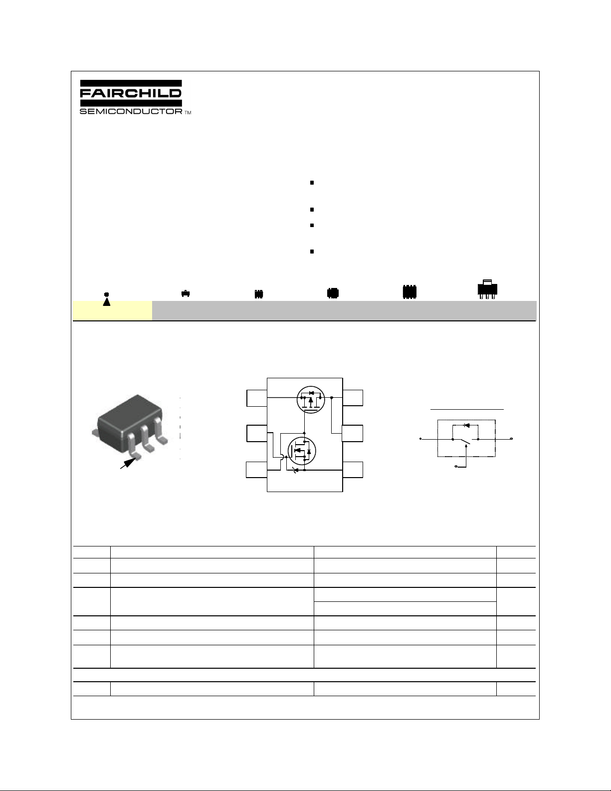
Integrated Load Switch
General Description Features
This device is intended to be configured as a load switch and
is particularly suited for compact computer peripheral
switching applications where 3V to 20V input and 0.6A output
current capability are needed. This device features a small
N-Channel MOSFET (Q1) together with a large P-Channel
Power MOSFET (Q2) in a single SC70-6 package.
V
DROP
VIN=5V, IL=0.27A. R
Very small package outline (SC70-6).
Control MOSFET (Q1) includes Zener protection for ESD
ruggedness (>6KV Human Body Model).
High density cell design for extremely low on-resistance.
=0.2V @ VIN=12V, IL=0.36A. R
= 0.75Ω.
(ON)
= 0.55Ω. V
(ON)
June 1999
=0.2V @
DROP
SC70-6 SuperSOTTM-6
SOT-23
SuperSOTTM-8
SO-8
SOT-223
V , C
OUT
V , COUT 1
R2
1
EQUIVALENT APPLICATION
IN
ON/OFF
V
DROP
+
-
pin 1
.24
V , R
IN
V
ON/OFF
R , C1
1
1
4
Q2
5
Q1
6
3
2
1
SC70-6
Absolute Maximum Ratings T
Symbol Parameter FDG6324L Units
V
IN
V
ON/OFF
I
L
P
D
TJ,T
ESD Electrostatic Discharge Rating
THERMAL CHARACTERISTICS
R
θJA
Input Voltage Range 3 - 20 V
On/Off Voltage Range 2.5 - 8 V
Load Current - Continuous (Note 1) 0.6 A
- Pulsed (Note 1 & 3) 1.8
Maximum Power Dissipation (Note 2) 0.3 W
Operating and Storage Temperature Range -55 to 150 °C
STG
Human Body Model (100pf/1500Ohm)
Thermal Resistance, Junction-to-Ambient (Note 2) 415 °C/W
= 25°C unless otherwise noted
A
6 kV
OUT
FDG6324L Rev.D

Electrical Characteristics (T
= 25°C unless otherwise noted)
A
Symbol Parameter Conditions Min Typ Max Units
OFF CHARACTERISTICS
I
FL
Forward Leakage Current
VIN = 20 V, V
ON/OFF
= 0 V
1 µA
ON CHARACTERISTICS (Note 3)
V
R
DROP
(ON)
Conduction Voltage Drop
VIN = 12 V, V
VIN = 5 V, V
= 3.3 V, IL = 0.36 A
ON/OFF
= 3.3 V, IL = 0.27 A
ON/OFF
Q2 - Static On-Resistance VGS = -12 V, ID = -0.6 A
VGS = -5 V, ID = -0.5 A
I
L
Notes:
1. Range of Vin can be up to 25V, but R1 and R2 must be scaled such that VGS of Q2 does not exceed -20V.
2. R
θJA
guaranteed by design while R
3. Pulse Test: Pulse Width < 300µs, Duty Cycle < 2.0%
Load Current
is the sum of the junction-to-case and case-to-ambient thermal resistance where the case thermal reference is defined as the solder mounting surface of the drain pins. R
is determined by the user's board design. Thermal ratings based on minimum mounting pad.
θCA
V
= 0.2 V, VIN = 12 V, V
DROP
V
= 0.2 V, VIN = 5 V, V
DROP
ON/OFF
ON/OFF
= 3.3 V
= 3.3 V
0.14 0.2 V
0.16 0.2
0.37 0.55
0.58 0.75
0.36 A
0.27
is
θJC
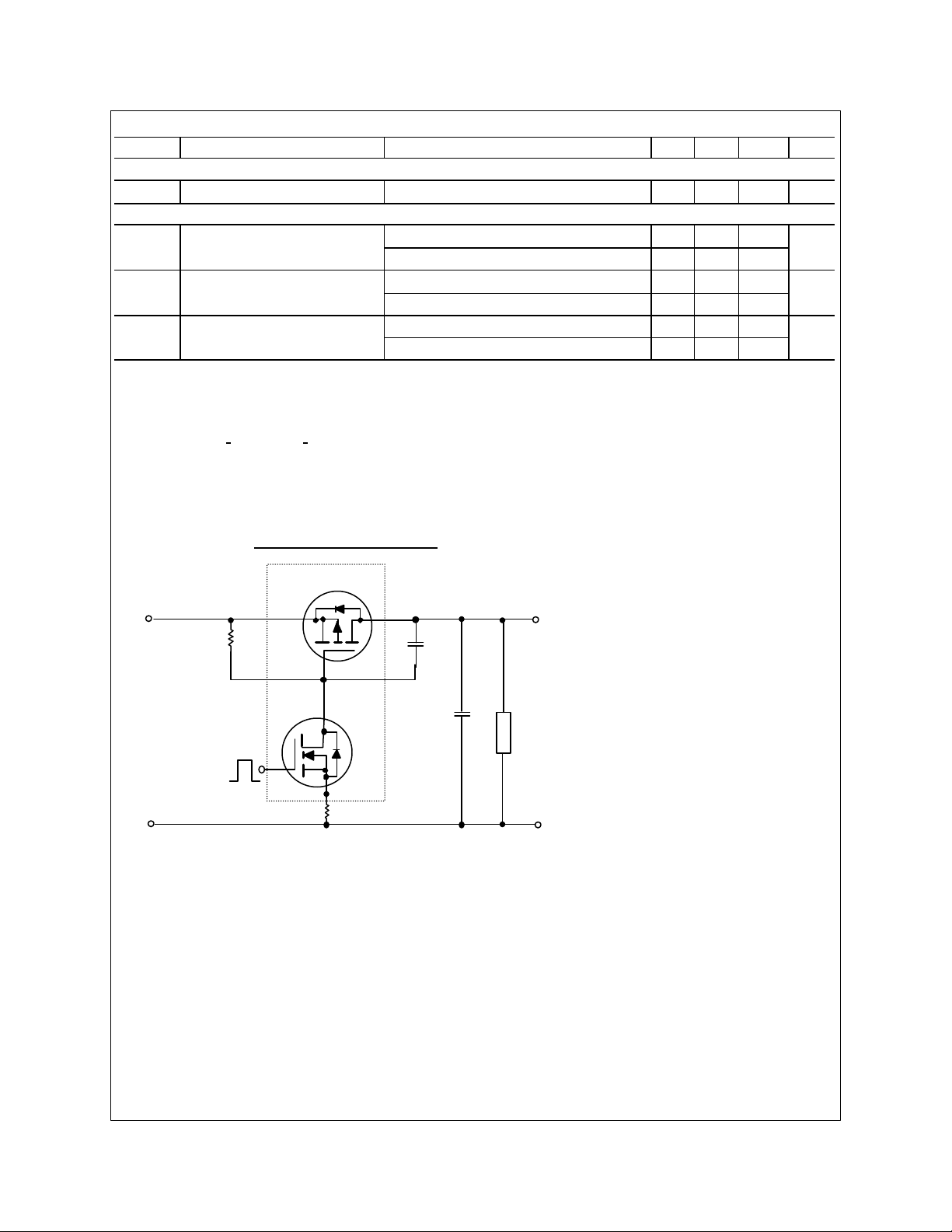
FDG6324L Load Switch Application
APPLICATION CIRCUIT
Ω
Q2
IN OUT
R1
Q1
ON/OFF
R2
External Component Recommendation
For Co ≤ 1uF applications:
R1 is required to turn Q2 off.
R2 and C1 are optional for slew rate control.
First select R2, 100 -1KΩ, for slew rate control.
Then select R1 such that the ratio R1/R2 is maintained between 10-100.
SPICE model (FDG6324L.MOD) available at www.fairchildsemi.com.
C1
Co
LOAD
FDG6324L Rev.D
 Loading...