FDG6318PZ
Dual P-Channel, Digital FET
FDG6318PZ
January 2003
General Description
These dual P-Channel logic level enhancement mode
MOSFET are produced using Fairchild Semiconductor’s
especially tailored to minimize on-state resistance. This
device has been designed especially for bipolar digital
transis t o r s an d sm al l si gnal MOSFETS
Applications
• Battery management
Features
• -0.5A, -20V. r
r
• Very low level gate drive requirements allowing direct
operation in 3V circuits (V
• Gate-Sou rce Z ene r f o r E SD ru gg ednes s ( >1.4 kV Huma n
Body Model).
• Compact industry standard SC-70-6 surface mount
package.
= 780mΩ (Max)@ VGS = -4.5 V
DS(ON)
= 1200mΩ (Max) @ VGS = -2.5 V
DS(ON)
< 1.5V).
GS(TH)
S
G
D
D
Pin 1
SC70-6
MOSFET Maximum Ratings T
Symbol Parameter Ratings Units
V
DSS
V
GS
I
D
P
D
, T
T
J
ESD
STG
Drain to Sou r c e Voltage -20 V
Gate to Source Voltage ±12 V
Drain Curr e nt
Continuous (T
Continuous (T
Pulsed Figure 4
Power dissipation 0.3 W
Derate above 25°C 2.4 mW/
Operating an d Stora ge Temperat ure -55 to 150
Electrostatic Discharge Rating MIL-STD -883D
Human Body Model ( 100pF / 1500Ω )
G
S
The pinouts are symmetri cal; pin1 and pin 4 are int erchangeable.
=25° C unless otherwise noted
A
= 25oC, VGS = - 4.5V)
C
= 100oC, VGS = - 2.5V) -0.3 A
C
S
G
D
1or4
2or5
3or6
D
6or3
G
5or2
S
4or1
-0.5 A
1.4 kV
o
C
o
C
Thermal Characteristics
R
θJA
Thermal Resistance Junction to Ambient (Note 1) 415
Package Marking and Ordering Information
Device Marking Device Package Reel Size Tape Width Quantity
.68 FDG6318PZ SC70-6 7” 8 mm 3000
©2003 FairchildSemiconductor Corporation
o
C/W
FDG6318PZ Rev. B

FDG6318PZ
Electrical Characteristics T
= 25°C unless otherwise noted
A
Symbol Parameter Test Conditions Min Typ Max Units
Off Characteristics
B
I
DSS
I
GSS
VDSS
Drain to Sou r c e Br ea k down Voltage ID = -250µA, VGS = 0V - 20 - - V
Zero Gate Voltage Drain Current V
= −16V , V
GS
= 0V - - -3 µA
GS
Gate to Source Leakage Current VGS = ±12V , VGS = 0V - - ±10 µA
On Characteristics
V
GS(TH)
r
DS(ON)
Gate to Source Threshold Voltage VGS = VDS, ID = -250µA -0.65 -0.9 -1.5 V
Drain to Source On Resistance
I
= -0.5A, V
D
= -0.4A, V
I
D
= -4.5V - 580 780
GS
= -2.5V - 910 1200
GS
Dynamic Characteristics
C
ISS
C
OSS
C
RSS
Q
g(TOT)
Q
g(-2.5)
Q
gs
Q
gd
Input Capacitance
Output Capacitance - 24.9 - pF
Reverse Transfer Capacitance - 8.83 - pF
Total Gate Charge at -4.5V VGS = 0V to -4.5V
Total Gate Charge at -2.5V VGS = 0V to -2.5V - 0.67 1.0 nC
Gate to Source Gate Charg e - 0.21 - nC
Gate to Drain “Miller” Charge - 0.33 - nC
Switching Characteristics
t
ON
t
d(ON)
t
r
t
d(OFF)
t
f
t
OFF
Turn-On Time
Turn-On Delay Time - 10 - ns
Rise Time - 13 - ns
Turn-Of f Delay Time - 40 - ns
Fall Time - 24 - ns
Turn-Of f Tim e - - 96 ns
(VGS = -4.5V)
= -10V , VGS = 0V,
V
DS
f = 1MHz
= -10V, ID = -0.5A
V
DD
V
= -4.5V, RGS = 120Ω
GS
V
DD
I
= -0.5A
D
I
= 1.0mA
g
= -10V
-85.4- pF
- 1.08 1.62 nC
- - 35 ns
mΩ
Drain-Source Diode Characteristics
V
SD
t
rr
Q
RR
Notes:
1. R
the center drain pad. R
©2003 Fairchild Semiconductor Corporation FDG6318PZ Rev. B
Source to Drain Diode Voltage I
Reverse Recovery Time ISD = -0.5A, dISD/dt = 100A/µs- -22ns
Reverse Recovered Charge ISD = -0.5A, dISD/dt = 100A/µs- -16nC
is the sum of the junction-to-case and case-to-ambient thermal resistance where the case thermal reference is defined as the solder mounting surface of
θJA
is guaranteed by design while R
θJC
θCA
= -0.5A - -0.9 -1.2 V
SD
is determined by user’s board design. R
415 oC/W when mounted on a 1inch2 copper pad.
θJA =

Typical Characteristic T
= 25°C unless otherwise noted
A
FDG6318PZ
1.2
1.0
0.8
0.6
0.4
0.2
POWER DISSIPATION MULTIPLIER
0
0 255075100 150
125
TA, AMBIENT TEMPERATURE (oC)
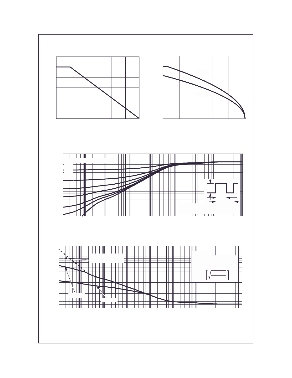
Figure 1. Normalized Power Dissipation vs
Ambient Temperature
2
DUTY CYCLE - DESCENDING ORDER
1
0.5
0.2
0.1
0.05
0.02
0.01
0.1
, NORMALIZED
θJA
Z
THERMAL IMPEDANCE
0.01
-5
10
-4
10
-3
10
10
t, RECTANGULAR PULSE DURATION (s)
0.6
V
= -4.5V
GS
0.4
V
= -2.5V
0.2
, DRAIN CURRENT (A)
D
-I
GS
0
25 50 75 100 125 150
TA, CASE TEMPERATURE (oC)
Figure 2. Maximum Continuous Drain Curr ent vs
Case Temperature
P
DM
t
1
t
θJA
+ T
10
2
A
2
3
10
NOTES:
DUTY FACTOR: D = t1/t2
PEAK T
= PDM x Z
J
-2
-1
10
0
10
x R
θJA
1
10
Figure 3. Normalized Maximum Transient Thermal Impedance
20
10
TRANSCONDUCTANCE
MAY LIMIT CURRENT
IN THIS REGION
TA = 25oC
FOR TEMPERATURES
o
ABOVE 25
C DERATE PEAK
CURRENT AS FOLLOWS:
150 - T
I = I25
A
125
, PEAK CURRENT (A)
DM
1
-I
VGS = -4.5V
VGS = -2.5V
0.4
-5
10
-4
10
-3
10
-2
10
-1
10
0
10
1
10
2
10
3
10
t, PULSE WIDTH (s)
Figure 4. Peak Current Capability
©2003 Fairchild Semiconductor Corporation FDG6318PZ Rev. B
 Loading...