Fairchild FDG1024NZ service manual

FDG1024NZ
Dual N-Channel PowerTrench® MOSFET
20 V, 1.2 A, 175 mΩ
Features
Max r
Max r
Max r
Max r
HBM ESD protection level >2 kV (Note 3)
Very low level gate drive requirements allowing operation in
1.5 V circuits (V
Very small package outline SC70-6
RoHS Compliant
= 175 mΩ at VGS = 4.5 V, ID = 1.2 A
DS(on)
= 215 mΩ at VGS = 2.5 V, ID = 1.0 A
DS(on)
= 270 mΩ at VGS = 1.8 V, ID = 0.9 A
DS(on)
= 389 mΩ at VGS = 1.5 V, ID = 0.8 A
DS(on)
< 1 V)
GS(th)
General Description
This dual N-Channel logic level enhancement mode field effect
transistors are produced using Fairchild’s proprietary, high cell
density, DMOS technology. This very high density process is
especially tailored to minimize on-state resistance. This device
has been designed especially for low voltage applications as a
replacement for bipolar digital transistors and small signal
MOSFETs. Since bias resistors are not required, this dual digital
FET can replace several different digital transistors, with
different bias resistor values.
FDG1024NZ Dual N-Channel Power Trench
June 2010
®
MOSFET
D1
G2
S2
S1
G1
1
2
6
5
D1
G2
D2
S1
G1
D2
3
4
S2
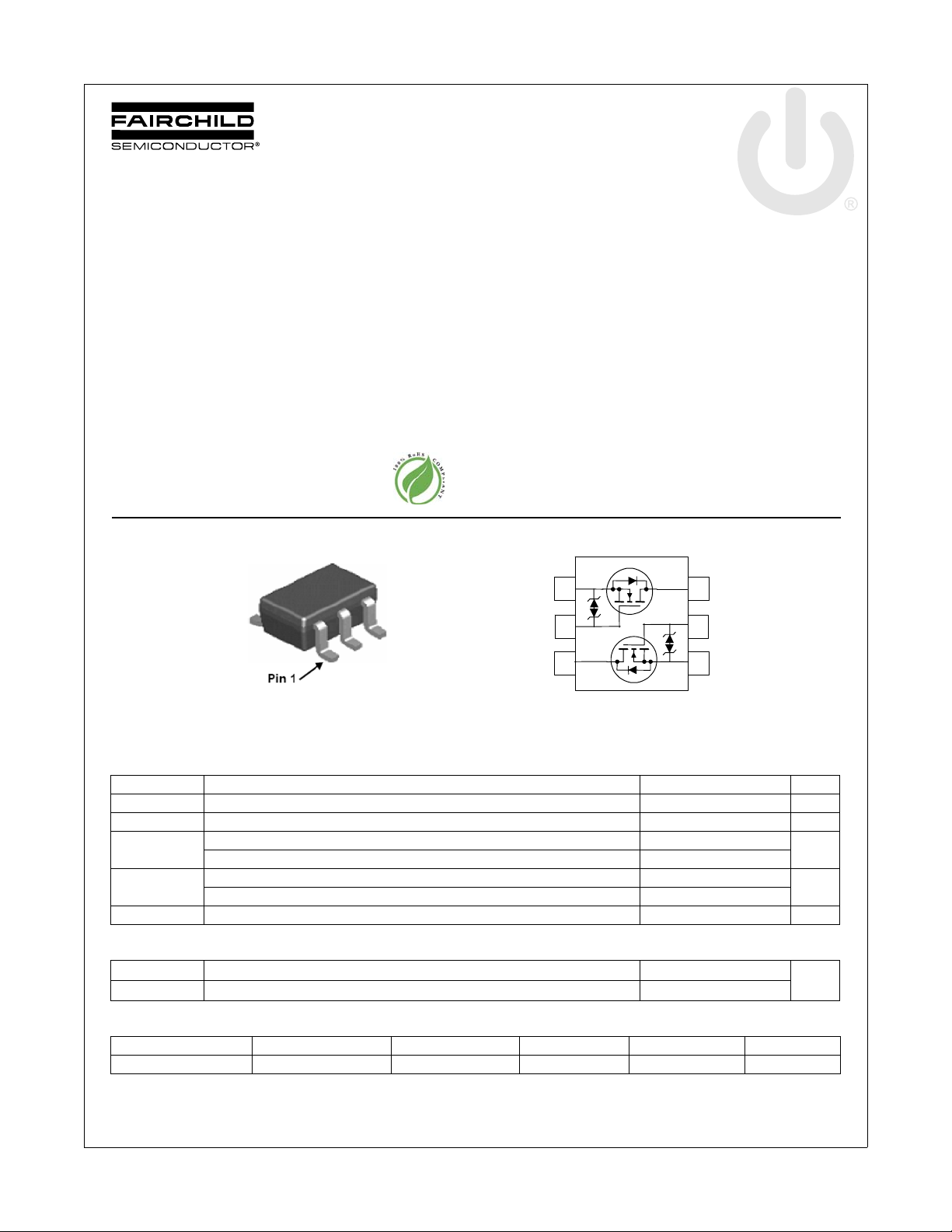
SC70-6
MOSFET Maximum Ratings T
Symbol Parameter Ratings Units
V
DS
V
GS
I
D
P
D
, T
T
J
STG
Drain to Source Voltage 20 V
Gate to Source Voltage ±8 V
-Continuous TA = 25°C (Note 1a) 1.2
-Pulsed 6
Power Dissipation TA = 25°C (Note 1a) 0.36
Power Dissipation T
Operating and Storage Junction Temperature Range -55 to +150 °C
= 25 °C unless otherwise noted
A
= 25°C (Note 1b) 0.30
A
Thermal Characteristics
R
θJA
R
θJA
Thermal Resistance, Junction to Ambient (Note 1a) 350
Thermal Resistance, Junction to Ambient (Note 1b) 415
Package Marking and Ordering Information
A
W
°C/W
Device Marking Device Package Reel Size Tape Width Quantity
.4N FDG1024NZ SC70-6 7 ” 8 mm 3000 units
©2010 Fairchild Semiconductor Corporation
FDG1024NZ Rev.C
1
www.fairchildsemi.com

Electrical Characteristics T
= 25 °C unless otherwise noted
J
Symbol Parameter Test Conditions Min Typ Max Units
Off Characteristics
BV
∆BV
∆T
I
DSS
I
GSS
DSS
DSS
J
Drain to Source Breakdown Voltage ID = 250 µA, VGS = 0 V 20 V
Breakdown Voltage Temperature
Coefficient
Zero Gate Voltage Drain Current VDS = 16 V, V
Gate to Source Leakage Current VGS = ±8 V, V
I
= 250 µA, referenced to 25 °C 14 mV/°C
D
= 0 V 1 µA
GS
= 0 V ±10 µA
DS
On Characteristics
V
GS(th)
∆V
∆T
r
DS(on)
g
FS
GS(th)
J
Gate to Source Threshold Voltage VGS = VDS, ID = 250 µA 0.4 0.8 1.0 V
Gate to Source Threshold Voltage
Temperature Coefficient
Static Drain to Source On Resistance
I
= 250 µA, referenced to 25 °C -3 mV/°C
D
V
= 4.5 V, ID = 1.2 A 160 175
GS
= 2.5 V, ID = 1.0 A 185 215
V
GS
= 1.8 V, ID = 0.9 A 232 270
V
GS
= 1.5 V, ID = 0.8 A 321 389
V
GS
= 4.5 V, ID = 1.2 A,
V
GS
T
=125 °C
J
220 259
Forward Transconductance VDD = 5 V, ID = 1.2 A 4 S
Dynamic Characteristics
C
iss
C
oss
C
rss
R
g
Input Capacitance
Output Capacitance 25 35 pF
Reverse Transfer Capacitance 20 25 pF
= 10 V, VGS = 0 V,
V
DS
f = 1 MHz
Gate Resistance 4.6 Ω
115 150 pF
FDG1024NZ Dual N-Channel Power Trench
mΩ
®
MOSFET
Switching Characteristics
t
d(on)
t
r
t
d(off)
t
f
Q
Q
Q
g
gs
gd
Turn-On Delay Time
Rise Time 1.7 10 ns
Turn-Off Delay Time 11 19 ns
Fall Time 1.5 10 ns
Total Gate Charge
Gate to Source Charge 0.3 nC
Gate to Drain “Miller” Charge 0.4 nC
V
= 10 V, ID = 1.2 A,
DD
= 4.5 V, R
V
GS
V
= 4.5 V, VDD = 10 V,
GS
= 1.2 A
I
D
GEN
Drain-Source Diode Characteristics
I
S
V
SD
t
rr
Q
rr
NOTES:
1. R
is determined with the device mounted on a 1 in2 pad 2 oz copper pad on a 1.5 x 1.5 in. board of FR-4 m ateri al. R
θJA
the user's board design.
Maximum Continuous Drain-Source Diode Forward Current 0.3 A
Source to Drain Diode Forward Voltage V
Reverse Recovery Time
Reverse Recovery Charge 1.9 10 nC
a. 350 °C/W when mounted
2
on a 1 in
pad of 2 oz copper.
= 0 V, IS = 0.3 A (Note 2) 0.7 1.2 V
GS
= 1.2 A, di/dt = 100 A/µs
I
F
= 6 Ω
is guaranteed by design while R
θJC
b. 415 °C/W when mounted on a
minimum pad of 2 oz copper.
3.7 10 ns
1.8 2.6 nC
10 20 ns
is determined by
θJA
2. Pulse Test: Pulse Width < 300 µs, Duty cycle < 2.0%.
3: The diode connected between the gate and source serves only as protection against ESD. No gate overvoltage rating is implied.
10 Fairchild Semiconductor Corporation
©20
FDG1024NZ Rev.
C
2
www.fairchildsemi.com

Typical Characteristics T
= 25 °C unless otherwise noted
J
FDG1024NZ Dual N-Channel Power Trench
6
5
VGS = 4.5 V
VGS = 3.5 V
VGS = 2.5 V
4
PULSE DURATION = 80 µs
3
2
DRAIN CURRENT (A)
,
D
I
1
0
0 0.4 0.8 1.2 1.6 2.0
V
,
DRAIN TO SOURCE VOLTAGE (V)
DS
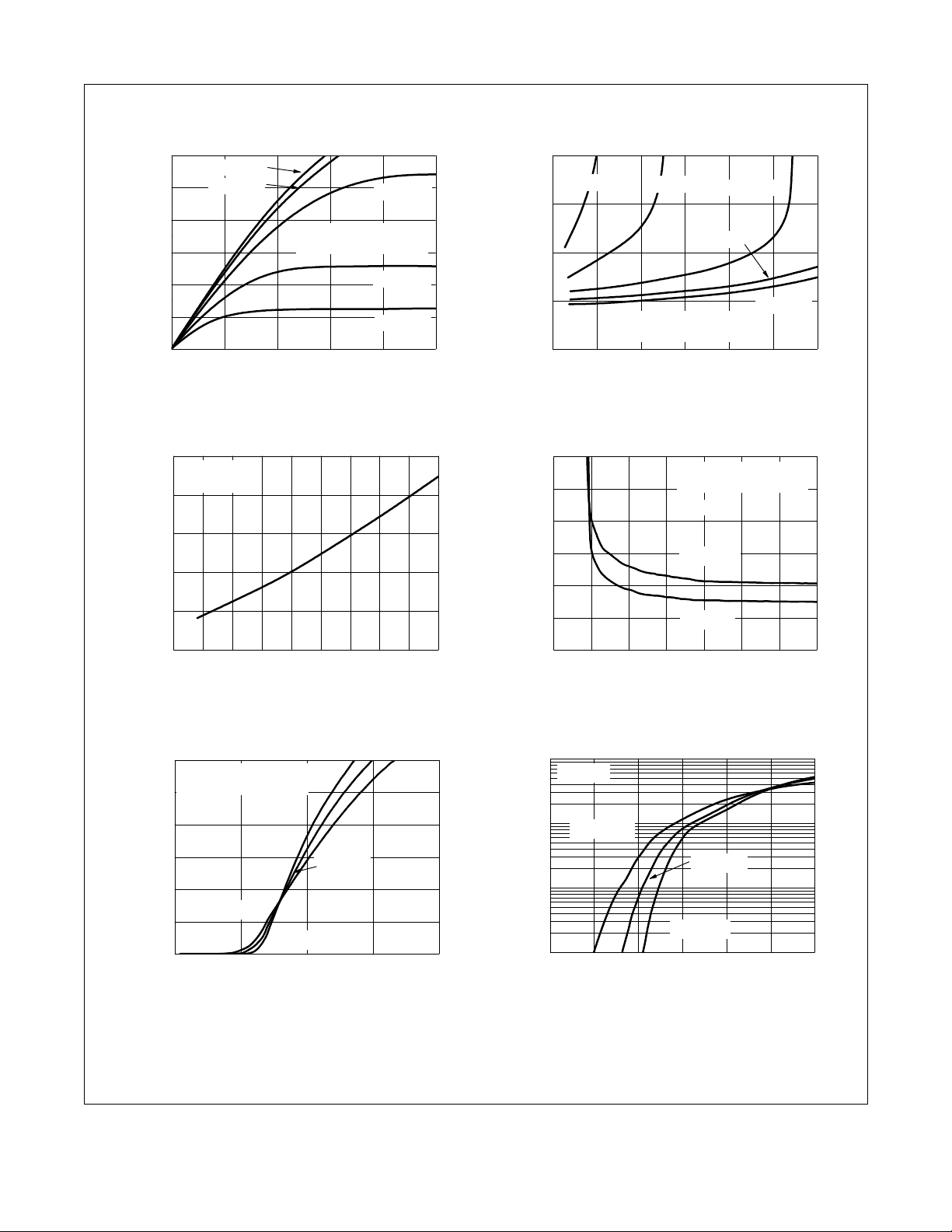
Figure 1.
1.6
ID = 1.2 A
V
1.4
On-Region Characteristics Figure 2.
= 4.5 V
GS
DUTY CYCLE = 0.5% MAX
VGS = 1.8 V
VGS = 1.5 V
1.2
1.0
NORMALIZED
0.8
DRAIN TO SOURCE ON-RESISTANCE
0.6
-75 -50 -25 0 25 50 75 100 125 150
T
,
JUNCTION TEMPERATURE
J
o
(
C
)
Figu r e 3. Norm a lized On - R esista n c e
vs Junction Temperature
2.5
V
GS
= 1.5 V
VGS = 1.8 V
V
= 2.5 V
GS
2.0
1.5
NORMALIZED
1.0
PULSE DURATION = 80 µs
DRAIN TO SOURCE ON-RESISTANCE
0.5
0123456
DUTY CYCLE = 0.5% MAX
I
,
DRAIN CURRENT (A)
D
VGS = 3.5 V
V
Norma l i z e d O n - Resistance
vs Drain Current and Gate Voltage
600
)
Ω
500
(m
400
300
DRAIN TO
,
200
DS(on)
r
100
SOURCE ON-RESISTANCE
0
1.01.52.02.53.03.54.04.5
V
,
GATE TO SOURCE VOLTAGE (V)
GS
Figure 4.
On-Resista nce vs Gate to
PULSE DURA TION = 80 µs
DUTY CYCLE = 0.5% MAX
ID = 1.2 A
TJ = 125 oC
TJ = 25 oC
Source Voltage
GS
= 4.5 V
®
MOSFET
6
PULSE DURATION = 80 µs
DUTY CYCLE = 0.5% MAX
5
V
= 5 V
DS
4
3
2
, DRAIN CURRENT (A)
D
I
TJ = 125 oC
1
0
01234
VGS, GATE TO SOURC E V OLTAGE (V)
Figure 5. Transfer Characteristics
10 Fairchild Semiconductor Corporation
©20
FDG1024NZ Rev.
C
TJ = -55 oC
TJ = 25 oC
10
V
= 0 V
GS
1
TJ = 125 oC
TJ = 25 oC
0.1
, REVERSE DRAIN CURRENT (A)
S
I
0.01
0.2 0.4 0.6 0.8 1.0 1.2 1.4
VSD, BODY DIODE FORWARD VOLTAGE (V)
Figure 6.
Source to Drain Diode
TJ = -55 oC
Forward Voltage vs Source Current
3
www.fairchildsemi.com
 Loading...