


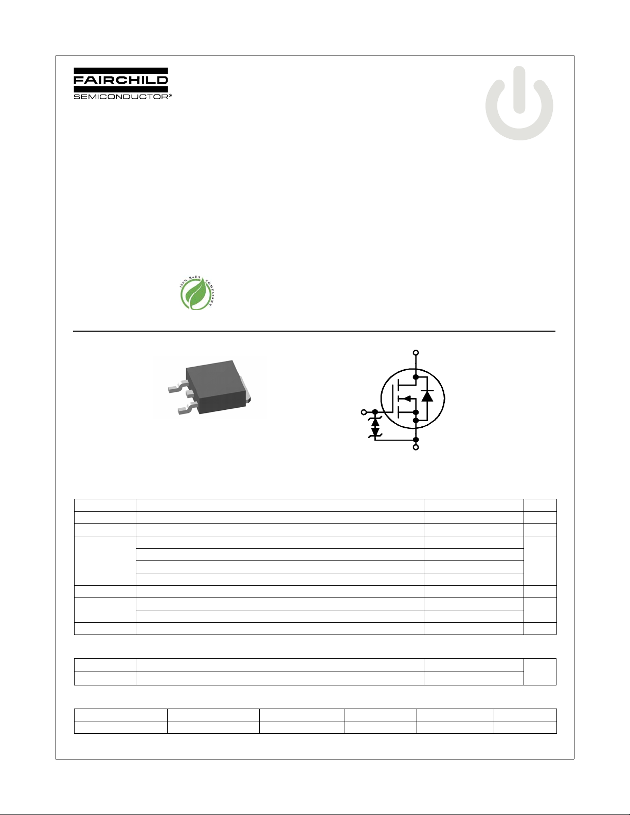
Fairchild FDD8453LZ service manual
tm
FDD8453LZ
(
)
N-Channel PowerTrench® MOSFET
40V, 50A, 6.7mΩ
Features
Max r
Max r
HBM ESD protection level >7kV typical (Note 4)
RoHS Compliant
= 6.7mΩ at VGS = 10V, ID = 15A
DS(on)
= 8.7mΩ at VGS = 4.5V, ID = 13A
DS(on)
General Description
This N-Channel MOSFET is produced using Fairchild
Semiconductor’s advanced PowerTrench
been especially tailored to minimize the on-state resistance and
switching loss. G-S zener has been added to enhance ESD
voltage level.
Applications
Inverter
Synchronous Rectifier
FDD8453LZ N-Channel PowerTrench
September 2007
®
process that has
®
MOSFET
D
D
G
S
D-PAK
TO-252
G
TO-252
S
MOSFET Maximum Ratings T
Symbol Parameter Ratings Units
V
DS
V
GS
I
D
E
AS
P
D
, T
T
J
STG
Thermal Characteristics
Drain to Source Voltage 40 V
Gate to Source Voltage ±20 V
Drain Current -Continuous (Package limited) TC = 25°C 50
-Continuous (Silicon limited) T
-Continuous T
-Pulsed 100
Single Pulse Avalanche Energy (Note 3) 253 mJ
Power Dissipation TC = 25°C 65
Power Dissipation T
Operating and Storage Junction Temperature Range -55 to +150 °C
= 25°C unless otherwise noted
C
= 25°C 75
C
= 25°C (Note 1a) 16.4
A
= 25°C (Note 1a) 3.1
A
A
W
R
θJC
R
θJA
Thermal Resistance, Junction to Case 1.9
Thermal Resistance, Junction to Ambient (Note 1a) 40
Package Marking and Ordering Information
Device Marking Device Package Reel Size Tape Width Quantity
FDD8453LZ FDD8453LZ D-PAK (TO-252) 13’’ 12mm 2500 units
©2007 Fairchild Semiconductor Corporation
FDD8453LZ Rev.C
°C/W
1
www.fairchildsemi.com
FDD8453LZ N-Channel PowerTrench
Electrical Characteristics T
= 25°C unless otherwise noted
J
Symbol Parameter Test Conditions Min Typ Max Units
Off Characteristics
BV
DSS
∆BV
DSS
∆T
J
I
DSS
I
GSS
On Characteristics
V
GS(th)
∆V
GS(th)
∆T
J
r
DS(on)
g
FS
Drain to Source Breakdown Voltage ID = 250µA, VGS = 0V 40 V
Breakdown Voltage Temperature
Coefficient
Zero Gate Voltage Drain Current VDS = 32V, V
Gate to Source Leakage Current VGS = ±20V, V
ID = 250µA, referenced to 25°C 36 mV/°C
= 0V 1 µA
GS
= 0V ±10 µA
DS
Gate to Source Threshold Voltage VGS = VDS, ID = 250µA 1.0 1.8 3.0 V
Gate to Source Threshold Voltage
Temperature Coefficient
Static Drain to Source On Resistance
Forward Transconductance VDS = 5V, ID = 15A 77 S
ID = 250µA, referenced to 25°C -6.0 mV/°C
VGS = 10V, ID = 15A 5.8 6.7
VGS = 4.5V, ID = 13A 6.8 8.7
VGS = 10V, ID = 15A,
TJ = 125°C
9.1 10.6
Dynamic Characteristics
C
iss
C
oss
C
rss
R
g
Input Capacitance
Output Capacitance 320 425 pF
Reverse Transfer Capacitance 190 285 pF
VDS = 20V, VGS = 0V,
f = 1MHz
2640 3515 pF
Gate Resistance f = 1MHz 2.3 Ω
mΩ
®
MOSFET
Switching Characteristics
t
d(on)
t
r
t
d(off)
t
f
Q
Q
Q
Q
g
g
gs
gd
Turn-On Delay Time
Rise Time 6 12 ns
Turn-Off Delay Time 37 58 ns
VDD = 20V, ID = 15A,
VGS = 10V, R
GEN
= 6Ω
11 19 ns
Fall Time 5 10 ns
Total Gate Charge V
Total Gate Charge V
Gate to Source Charge 7 nC
= 0V to 10V
GS
= 0V to 5V 24 33 nC
GS
VDD = 20V,
ID = 15A
46 64 nC
Gate to Drain “Miller” Charge 8 nC
Drain-Source Diode Characteristics
V
= 0V, IS = 2.0A (Note 2) 0.7 1.2
V
SD
t
rr
Q
rr
Notes:
1: R
R
θJA
θJC
Source to Drain Diode Forward Voltage
Reverse Recovery Time
Reverse Recovery Charge 20 32 nC
is the sum of the junction-to-case and case-to-ambient thermal resistance where the case thermal reference is defined as the solder mounting surface of the drain pins.
is guaranteed by design while R
is determined by the user’s board design.
θJA
a)
40°C/W when mounted on a
2
1 in
pad of 2 oz copper
GS
V
= 0V, IS = 15A (Note 2) 0.8 1.3
GS
IF = 15A, di/dt = 100A/µs
b)
25 40 ns
96°C/W when mounted
on a minimum pad.
V
2: Pulse Test: Pulse Width < 300µs, Duty cycle < 2.0%.
3: Starting T
4: The diode connected between the gate and source serves only as protection against ESD. No gate overvoltage rating is implied.
©2007 Fairchild Semiconductor Corporation
FDD8453LZ Rev.C
= 25°C, L = 3mH, IAS = 13A, VDD = 40V, VGS = 10V.
J
www.fairchildsemi.com2
FDD8453LZ N-Channel PowerTrench
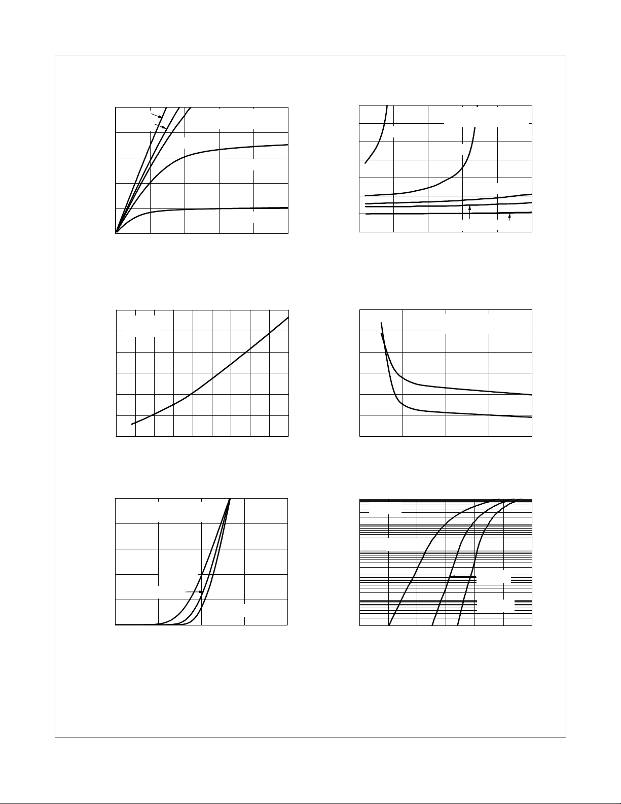
Typical Characteristics T
100
VGS = 10V
VGS = 4.5V
80
60
40
, DRAIN CURRENT (A)
D
I
20
0
0.0 0.4 0.8 1.2 1.6 2.0
VDS, DRAIN TO SOURCE VOLTAGE (V)
Figure 1.
On-Region Characteristics Figure 2.
1.8
ID = 15A
V
GS
= 10V
1.6
1.4
1.2
1.0
NORMALIZED
0.8
DRAIN TO SOURCE ON-RESISTANCE
0.6
-75 -50 -25 0 25 50 75 100 125 150
T
, JUNCTION TEMPERATURE (
J
Figu r e 3. Norm a l ized On - R esista n c e
vs Junction Temperature
PULSE DURATION = 80µs
DUTY CYCLE = 0.5%MAX
VGS = 4V
= 25°C unless otherwise noted
J
VGS = 3.5V
VGS = 3V
o
C)
4.0
3.5
3.0
VGS = 3V
PULSE DURATION = 80µs
DUTY CYCLE = 0.5%MAX
VGS = 3.5V
2.5
2.0
NORMALIZED
1.5
VGS = 4V
1.0
V
DRAIN TO SOURCE ON-RESISTANCE
0.5
020406080100
I
, DRAIN CURRENT (A)
D
VGS = 4.5V
GS
= 10V
Norma l i z e d O n - R esistance
vs Drain Current and Gate Voltage
21
18
ID = 15A
(mΩ)
15
12
, DRAIN TO
9
DS(on)
r
6
SOURCE ON-RESISTANCE
3
246810
VGS, GATE TO SOURCE VOLTA G E (V)
Figure 4.
On-Resis tance vs Gate to
PULSE DURATION = 80µs
DUTY CYCLE = 0.5%MAX
TJ = 125oC
o
T
= 25
C
J
Source Voltage
®
MOSFET
100
PULSE DURATION = 80µs
DUTY CYCLE = 0.5%MAX
80
V
= 5V
DS
60
40
, DRAIN CURRENT (A)
20
D
I
0
12345
TJ = 150oC
TJ = 25oC
VGS, GATE TO SOURCE VOLTAGE (V)
Figure 5. Transfer Characteristics
©2007 Fairchild Semiconductor Corporation
FDD8453LZ Rev.C
TJ = -55oC
100
V
= 0V
GS
10
1
0.1
0.01
, REVERSE DRAIN CURRENT (A)
S
I
1E-3
0.0 0.2 0.4 0.6 0.8 1.0 1.2
TJ = 150oC
VSD, BODY DIODE FORWARD VOLTAGE (V)
Figure 6.
Source to Drain Diode
TJ = 25oC
TJ = -55oC
Forward Voltage vs Source Current
www.fairchildsemi.com3