tm
FDD8445
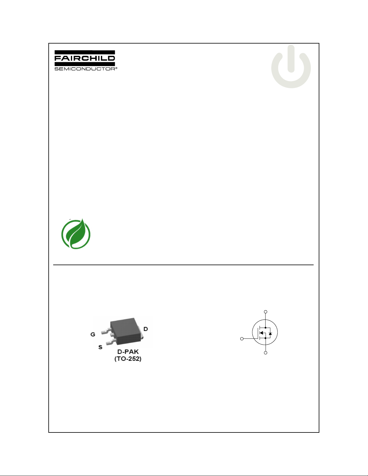
D
G
S
N-Channel PowerTrench® MOSFET
40V, 50A, 8.7mΩ
FDD8445 N-Channel PowerTrench
March 2007
Features
R
Q
Low Miller Charge
Low Qrr Body Diode
UIS Capability (Single Pulse/ Repetitive Pulse)
Qualified to AEC Q101
RoHS Compliant
= 6.7 mΩ (Typ), VGS = 10V, ID=50A
DS(ON)
= 45nC (Typ), VGS=10V
g(10)
E
E
R
F
I
D
A
E
L
M
P
L
E
M
E
N
T
A
T
I
O
N
Applications
Automotive Engine Control
Powertrain Management
Solenoid and Motor Drivers
Electronic Transmission
Distributed Power Architecture and VRMs
Primary Switch for 12V Systems
®
MOSFET
©2007 Fairchild Semiconductor Corporation
FDD8445 Rev A (W)
www.fairchildsemi.com1

Absolute Maximum Ratings T
= 25°C unless otherwise noted
c
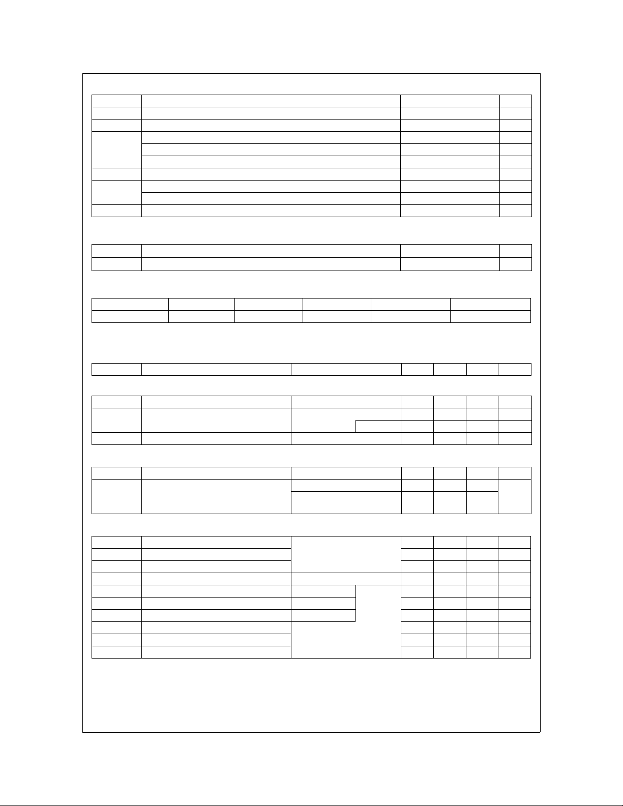
Symbol Parameter Ratings Units
V
DSS
V
GS
Drain to Source Voltage 40 V
Gate to Source Voltage ±20 V
Drain Current Continuous (VGS=10v) (Note 1) 70 A
I
D
Continuous (V
=10v,with R
GS
= 52oC/W) 15.2 A
θJA
Pulsed Figure 4
E
AS
P
D
, T
T
J
STG
S i n g l e P u l s e A v a l a n c h e E n e r g y ( N o t e 2 ) 1 4 4 mJ
Power Dissipation 79 W
o
Derate above 25
C0.53W/oC
Operating and Storage Temperature -55 to +175
Thermal Characteristics
R
θJC
R
θJA
Thermal Resistance, Junction to Case 1.9
Thermal Resistance, Junction to Ambient TO-252, lin2 copper pad area 52
Package Marking and Ordering Information
Device Marking Device Package Reel Size Tape Width Quantity
FDD8445 FDD8445 TO-252AA 13” 12mm 2500 units
o
C/W
o
C/W
FDD8445 N-Channel PowerTrench
o
C
®
MOSFET
Electrical Characteristics T
= 25°C unless otherwise noted
J
Symbol Parameter Test Conditions Min Typ Max Units
Off Characteristics
BV
I
DSS
I
GSS
DSS
Drain to Source Breakdown Voltage ID = 250μA, VGS = 0V 40 - - V
Zero Gate Voltage Drain Current
VDS = 32V
V
= 0V
GS
TJ=150°C - - 250
- - 1 μA
Gate to Source Leakage Current VGS = ±20V - - ±100 nA
On Characteristics
V
GS(th)
R
DS(ON)
Gate to Source Threshold Voltage VDS = VGS, ID = 250μA 2 2.8 4 V
ID = 50A, VGS = 10V - 6.7 8.7
Drain to Source On Resistance
ID = 50A, VGS = 10V,
TJ = 175°C
- 12.5 16.3
Dynamic Characteristics
C
ISS
C
OSS
C
RSS
R
G
Q
g(TOT)
Q
g(5)
Q
g(TH)
Q
gs
Q
gs2
Q
gd
Input Capacitance
Output Capacitance - 295 390 pF
Reverse Transfer Capacitance - 178 270 pF
VDS = 25V, VGS = 0V,
f = 1MHz
- 3040 4050 pF
Gate Resistance f = 1MHz - 1.7 - Ω
Total Gate Charge at 10V VGS = 0 to 10V
- 45 59 nC
Total Gate Charge at 5V VGS = 0 to 5V - 17 22 nC
Threshold Gate Charge VGS = 0 to 2V - 5.8 7.6 nC
Gate to Source Gate Charge
Gate Charge Threshold to Plateau - 9.5 - nC
VDD = 20V,
ID = 5 0 A
- 12.5 - nC
Gate to Drain “Miller” Charge - 10.5 - nC
mΩ
FDD8445 Rev A (W) www.fairchildsemi.com2

Electrical Characteristics T
= 25°C unless otherwise noted
J
Symbol Parameter Test Conditions Min Typ Max Units
Switching Characteristics
t
(on)
t
d(on)
t
r
t
d(off)
t
f
t
off
Turn-On Time
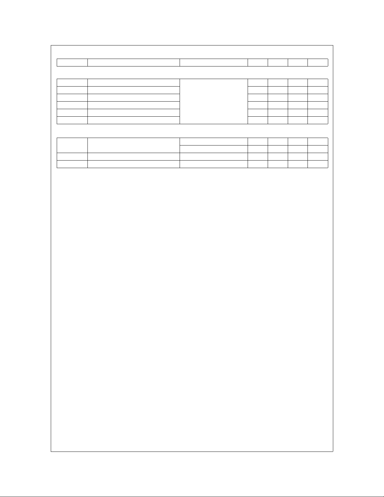
Turn-On Delay Time - 10 - ns
Turn-On Rise Time - 82 - ns
Turn-Off Delay Time - 26 - ns
V
= 20V, ID = 50A
DD
V
= 10V, RGS = 2Ω
GS
Turn-Off Fall Time - 9.6 - ns
Turn-Off Time - - 53 ns
- - 138 ns
Drain-Source Diode Characteristics
I
=50A - - 1.25 V
V
SD
t
rr
Q
rr
Notes:
1: Maximum package current capability is 50A.
2: Starting T
Source to Drain Diode Voltage
Reverse Recovery Time IF= 50A, dIF/dt=100A/μs--39ns
Reverse Recovery Charge IF= 50A, dIF/dt=100A/μs--38nC
= 25oC, L=0.18mH, IAS=40A.
J
SD
=25A - - 1.0 V
I
SD
FDD8445 N-Channel PowerTrench
®
MOSFET
This product has been designed to meet the extreme test conditions and environment demanded by the automotive industry. For
All Fairchild Semiconductor products are manufactured, assembled and tested under ISO9000 and QS9000 quality systems
FDD8445 Rev A (W) www.fairchildsemi.com3
a copy of the requirements, see AEC Q101 at: http://www.aecouncil.com/
certification.
 Loading...