Fairchild FDD8424H service manual

tm
FDD8424H
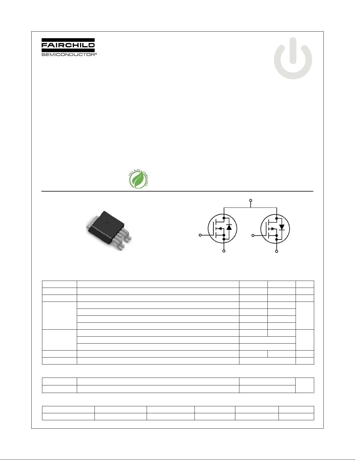
Dual N & P-Channel PowerTrench® MOSFET
N-Channel: 40V, 20A, 24mΩ P-Channel: -40V, -20A, 54mΩ
FDD8424H Dual N & P-Channel PowerTrench
March 2007
Features
Q1: N-Channel
Max r
Max r
Q2: P-Channel
Max r
Max r
Fast switching speed
RoHS Compliant
MOSFET Maximum Ratings T
Symbol Parameter Q1 Q2 Units
V
DS
V
GS
I
D
P
D
E
AS
, T
T
J
= 24mΩ at VGS = 10V, ID = 9.0A
DS(on)
= 30mΩ at VGS = 4.5V, ID = 7.0A
DS(on)
= 54mΩ at VGS = -10V, ID = -6.5A
DS(on)
= 70mΩ at VGS = -4.5V, ID = -5.6A
DS(on)
D1/D2
Dual DPAK 4L
Drain to Source Voltage 40 -40 V
Gate to Source Voltage ±20 ±20 V
Drain Current - Continuous (Package Limited) 20 -20
- Continuous (Silicon Limited) T
- Continuous T
- Pulsed 55 -40
Power Dissipation for Single Operation TC = 25°C (Note 1) 30 35
T
Single Pulse Avalanche Energy (Note 3) 29 33 mJ
STG
Operating and Storage Junction Temperature Range -55 to +150 °C
S1
G2
S2
G1
= 25°C unless otherwise noted
C
General Description
These dual N and P-Channel enhancement mode Power
MOSFETs are produced using Fairchild Semiconductor’s
advanced PowerTrench- process that has been especially
tailored to minimize on-state resistance and yet maintain
superior switching performance.
Application
Inverter
H-Bridge
G1
N-Channel P-Channel
= 25°C 26 -20
C
= 25°C 9.0 -6.5
A
= 25°C (Note 1a) 3.1
A
= 25°C (Note 1b) 1.3
A
D1 D2
G2
S1
S2
Thermal Characteristics
®
MOSFET
A
W T
R
θJC
R
θJC
Thermal Resistance, Junction to Case, Single Operation for Q1 (Note 1) 4.1
Thermal Resistance, Junction to Case, Single Operation for Q2 (Note 1) 3.5
Package Marking and Ordering Information
Device Marking Device Package Reel Size Tape Width Quantity
FDD8424H FDD8424H TO-252-4L 13” 12mm 2500 units
©2007 Fairchild Semiconductor Corporation
FDD8424H Rev.C
°C/W
1
www.fairchildsemi.com

FDD8424H Dual N & P-Channel PowerTrench
Electrical Characteristics T
= 25°C unless otherwise noted
J
Symbol Parameter Test Conditions Type Min Typ Max Units
Off Characteristics
BV
∆BV
∆T
I
DSS
I
GSS
DSS
DSS
J
Drain to Source Breakdown Voltage
Breakdown Voltage Temperature
Coefficient
Zero Gate Voltage Drain Current
Gate to Source Leakage Current VGS = ±20V, V
On Characteristics
V
GS(th)
∆V
∆T
r
DS(on)
g
FS
GS(th)
J
Gate to Source Threshold Voltage
Gate to Source Threshold Voltage
Temperature Coefficient
Static Drain to Source On Resistance
Forward Transconductance
ID = 250µA, VGS = 0V
ID = -250µA, VGS = 0V
ID = 250µA, referenced to 25°C
ID = -250µA, referenced to 25°CQ1Q2
VDS = 32V, V
VDS = -32V, V
GS
GS
DS
= 0V
= 0V
= 0V
VGS = VDS, ID = 250µA
VGS = VDS, ID = -250µA
ID = 250µA, referenced to 25°C
ID = -250µA, referenced to 25°C
VGS = 10V, ID = 9.0A
VGS = 4.5V, ID = 7.0A
VGS = 10V, ID = 9.0A, TJ = 125°C
VGS = -10V, ID = -6.5A
VGS = -4.5V, ID = -5.6A
VGS = -10V, ID = -6.5A, TJ = 125°C
VDS = 5V, ID = 9.0A
VDS = -5V, ID = -6.5A
Q1Q240
-40
Q1
Q2
Q1
Q2
Q1Q21
Q1
Q2
Q1
Q2
Q1
Q2
-1
V
34
-32
mV/°C
1
-1
±100
±100nAnA
1.7
-1.6
-5.3
4.8
19
23
29
42
58
62
3
-3
mV/°C
24
30
37
54
70
80
29
13
µA
V
mΩ
S
®
MOSFET
Dynamic Characteristics
C
iss
C
oss
C
rss
R
g
Input Capacitance
Output Capacitance
Reverse Transfer Capacitance
Gate Resistance f = 1MHz
Switching Characteristics
t
d(on)
t
r
t
d(off)
t
f
Q
g(TOT)
Q
gs
Q
gd
Turn-On Delay Time
Rise Time
Turn-Off Delay Time
Fall Time
Total Gate Charge
Gate to Source Charge
Gate to Drain “Miller” Charge
Q1
V
= 20V, VGS = 0V, f = 1MHZ
DS
Q2
V
= -20V, VGS = 0V, f = 1MHZ
DS
Q1
VDD = 20V, ID = 9.0A,
VGS = 10V, R
GEN
= 6Ω
Q2
VDD = -20V, ID = -6.5A,
VGS = -10V, R
GEN
= 6Ω
Q1
VGS = 10V, VDD = 20V, ID = 9.0A
Q2
VGS = -10V, VDD = -20V, ID = -6.5A
Q1
Q2
Q1
Q2
Q1
Q2
Q1
Q2
Q1
Q2
Q1
Q2
Q1
Q2
Q1
Q2
Q1
Q2
Q1
Q2
Q1
Q2
750
115
140
75
75
1.1
3.3
7
7
13
3
17
20
6
3
14
17
2.3
3.0
3.2
3.6
1000
1330
155
185
115
115
14
14
24
10
31
36
12
10
20
24
pF
pF
pF
Ω
ns
ns
ns
ns
nC
nC
nC
1000
©2007 Fairchild Semiconductor Corporation
FDD8424H Rev.C
2
www.fairchildsemi.com

FDD8424H Dual N & P-Channel PowerTrench
Electrical Characteristics T
= 25°C unless otherwise noted
J
Symbol Parameter Test Conditions Type Min Typ Max Units
Drain-Source Diode Characteristics
V
= 0V, IS = 9.0A (Note 2)
V
SD
t
rr
Q
rr
Notes:
1. R
is determined with the device mounted on a 1in2 pad 2 oz copper pad on a 1.5 x 1.5 in. board of FR-4 material. R
θJA
by the user's board design.
Source to Drain Diode Forward Voltage
Reverse Recovery Time
Reverse Recovery Charge
Q1
Q2
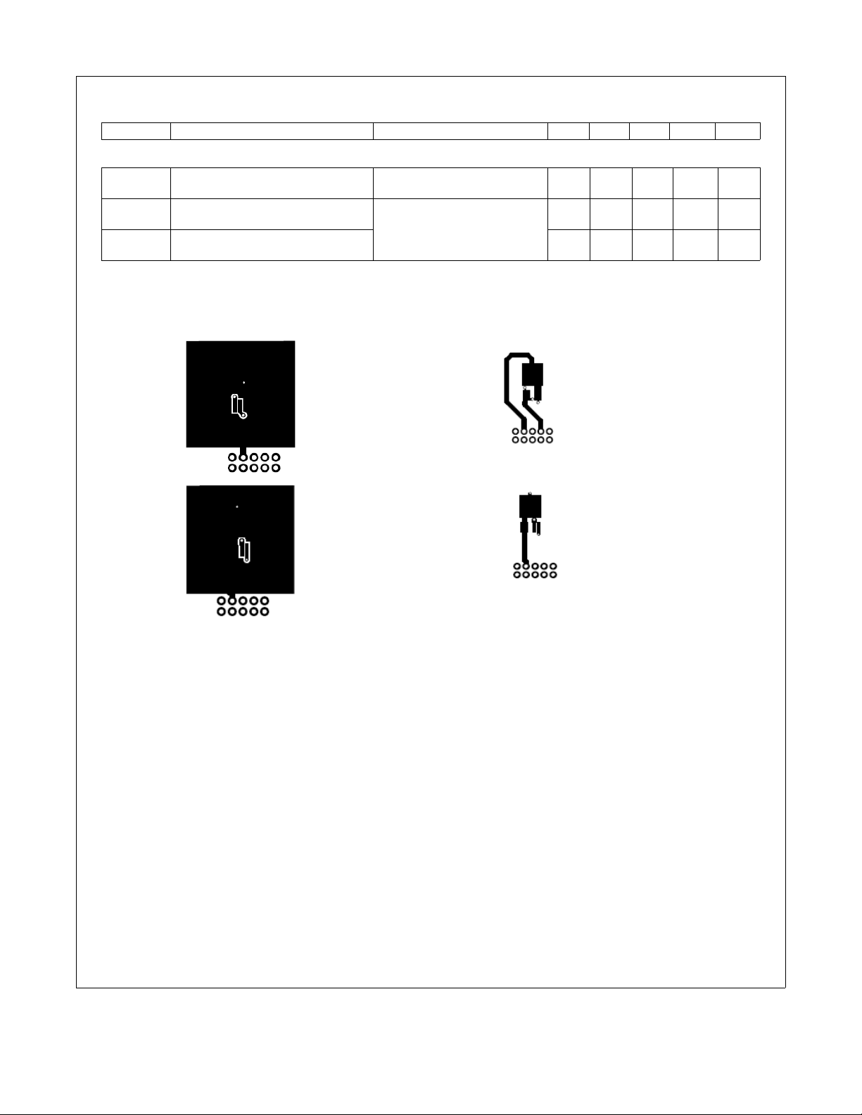
a. 40°C/W when mounted on
a 1 in
Scale 1 : 1 on letter size paper
a. 40°C/W when mounted on
a 1 in
2
2
GS
V
= 0V, IS = -6.5A (Note 2)Q1Q2
GS
Q1
I
= 9.0A, di/dt = 100A/s
F
Q2
I
= -6.5A, di/dt = 100A/s
F
pad of 2 oz copper
pad of 2 oz copper
0.87
0.88
Q1
Q2
Q1
Q2
is guaranteed by design while R
θJC
b. 96°C/W when mounted on a
minimum pad of 2 oz copper
b. 96°C/W when mounted on a
minimum pad of 2 oz copper
25
29
19
29
1.2
-1.2
38
44
29
44
is determined
θCA
V
ns
nC
®
MOSFET
Scale 1 : 1 on letter size paper
2. Pulse Test: Pulse Width < 300µs, Duty cycle < 2.0%.
3. Starting TJ = 25°C, N-ch: L = 0.3mH, IAS = 14A, VDD = 40V, VGS = 10V; P-ch: L = 0.3mH, IAS = -15A, VDD = -40V, VGS = -10V.
©2007 Fairchild Semiconductor Corporation
FDD8424H Rev.C
3
www.fairchildsemi.com

FDD8424H Dual N & P-Channel PowerTrench
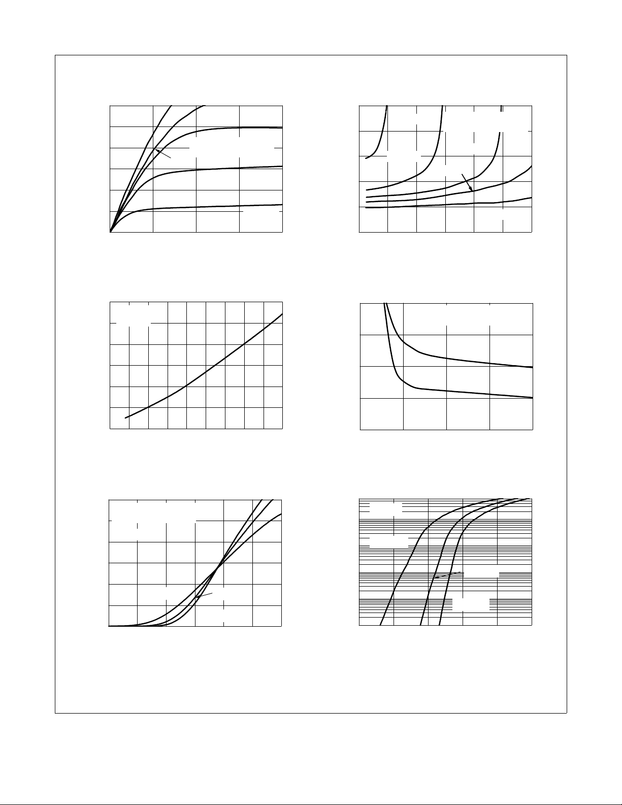
Typical Characteristics (Q1 N-Channel)T
60
50
VGS = 10V
40
30
VGS = 4.5V
PULSE DURATION = 80µs
DUTY CYCLE = 0.5%MAX
20
, DRAIN CURRENT (A)
D
I
10
0
01234
VDS, DRAIN TO SOURCE VOLTAGE (V)
Figure 1.
On- Region Characteristics Figure 2.
1.8
ID = 9A
V
= 10V
GS
1.6
1.4
1.2
1.0
NORMALIZED
0.8
DRAIN TO SOURCE ON-RESISTANCE
0.6
-75 -50 -25 0 25 50 75 100 125 150
TJ, JUNCTION TEMPERATURE (oC)
Fig ure 3. N ormalize d On -Re sis tan ce
vs Junction Temperature
VGS = 4.0V
VGS = 3.5V
VGS = 3.0V
= 25°C unless otherwise noted
J
3.0
VGS = 3.0V
2.5
V
GS
= 3.5V
NORMALIZED
2.0
1.5
1.0
DRAIN TO SOURCE ON-RESISTANCE
0.5
0 102030405060
ID, DRAIN CURRENT(A)
Nor mal i zed On- R esi sta n ce
vs Drain Current and Gate Voltage
50
(mΩ)
40
30
, DRAIN TO
DS(on)
r
20
SOURCE ON-RESISTANCE
10
246810
VGS, GATE TO SO URCE VOLT AGE ( V)
Figure 4.
On-Re sistance vs Gate to
Source Voltage
ID = 9A
PULSE DURATION = 80µs
DUTY CYCLE = 0.5%MAX
V
= 4.0V
GS
V
= 4.5V
GS
V
GS
PULSE DURATION = 80µs
DUTY CYCLE = 0.5%MAX
TJ = 125oC
o
T
= 25
C
J
= 10V
®
MOSFET
60
PULSE DURATION = 80µs
DUTY CYCLE = 0.5%MAX
50
V
= 5V
DS
40
30
20
, DRAIN CURRENT (A)
D
I
10
0
1.5 2.0 2.5 3.0 3.5 4.0 4.5
TJ = 150oC
VGS, GATE TO SOURCE VOLTAGE (V)
Figure 5. Transfer Characteristics
©2007 Fairchild Semiconductor Corporation
FDD8424H Rev.C
TJ = -55oC
TJ = 25oC
60
V
= 0V
GS
10
TJ = 150oC
1
0.1
0.01
, REVERSE DRAIN CURRENT (A)
S
I
0.001
0.0 0.3 0.6 0.9 1.2 1.5
VSD, BODY DIODE FORWARD VOLTAGE (V)
Figure 6.
Sourc e to Dr ain Di ode
TJ = 25oC
TJ = -55oC
Forward Voltage vs Source Current
4
www.fairchildsemi.com
 Loading...