

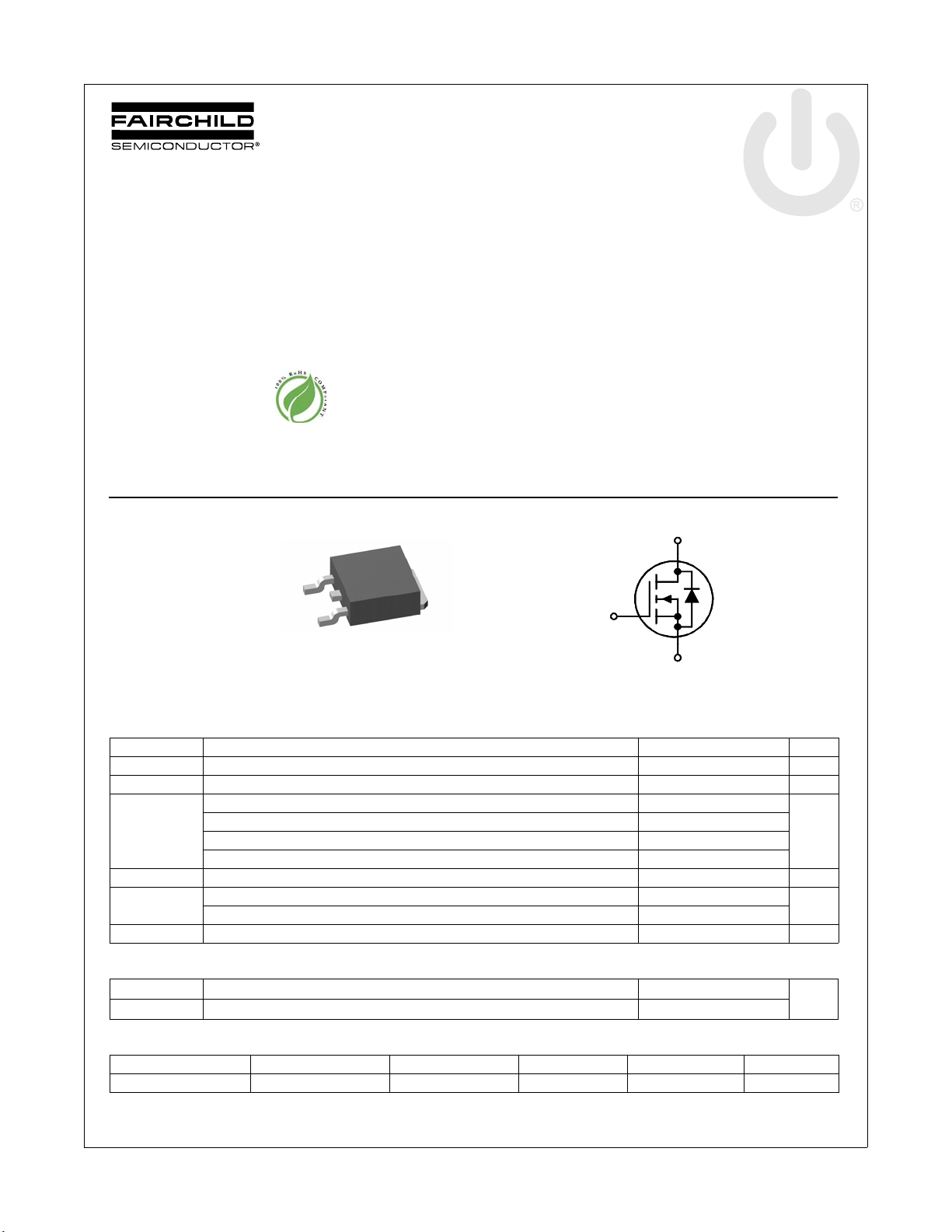
FDD6770A
(
)
N-Channel PowerTrench® MOSFET
25 V, 4.0 mΩ
Features
Max r
Max r
100% UIL tested
RoHS Compliant
= 4.0 mΩ at VGS = 10 V, ID = 24 A
DS(on)
= 8.0 mΩ at VGS = 4.5 V, ID = 18.4 A
DS(on)
General Description
This N-Channel MOSFET has been designed specifically to
improve the overall efficiency of DC/DC converters using either
synchronous or conventional switching PWM controllers. It has
been optimized for low gate charge, low r
switching speed.
Applications
Vcore DC-DC for Desktop Computers and Servers
VRM for Intermediate Bus Architecture
FDD6770A N-Channel PowerTrench
January 2009
and fast
DS(on)
®
MOSFET
D
G
D
G
S
D-PAK
TO-252
TO-252
MOSFET Maximum Ratings T
Symbol Parameter Ratings Units
V
DS
V
GS
I
D
E
AS
P
D
, T
T
J
STG
Drain to Source Voltage 25 V
Gate to Source Voltage ±20 V
Drain Current -Continuous (Package limited) TC = 25 °C 50
-Continuous (Silicon limited) T
-Continuous T
-Pulsed 200
Single Pulse Avalanche Energy (Note 3) 50 mJ
Power Dissipation TC = 25 °C 50
Power Dissipation T
Operating and Storage Junction Temperature Range -55 to +175 °C
= 25 °C unless otherwise noted
C
= 25 °C 97
C
= 25 °C (Note 1a) 24
A
= 25 °C (Note 1a) 3.7
A
S
Thermal Characteristics
R
θJC
R
θJA
Thermal Resistance, Junction to Case 3.0
Thermal Resistance, Junction to Ambient (Note 1a) 40
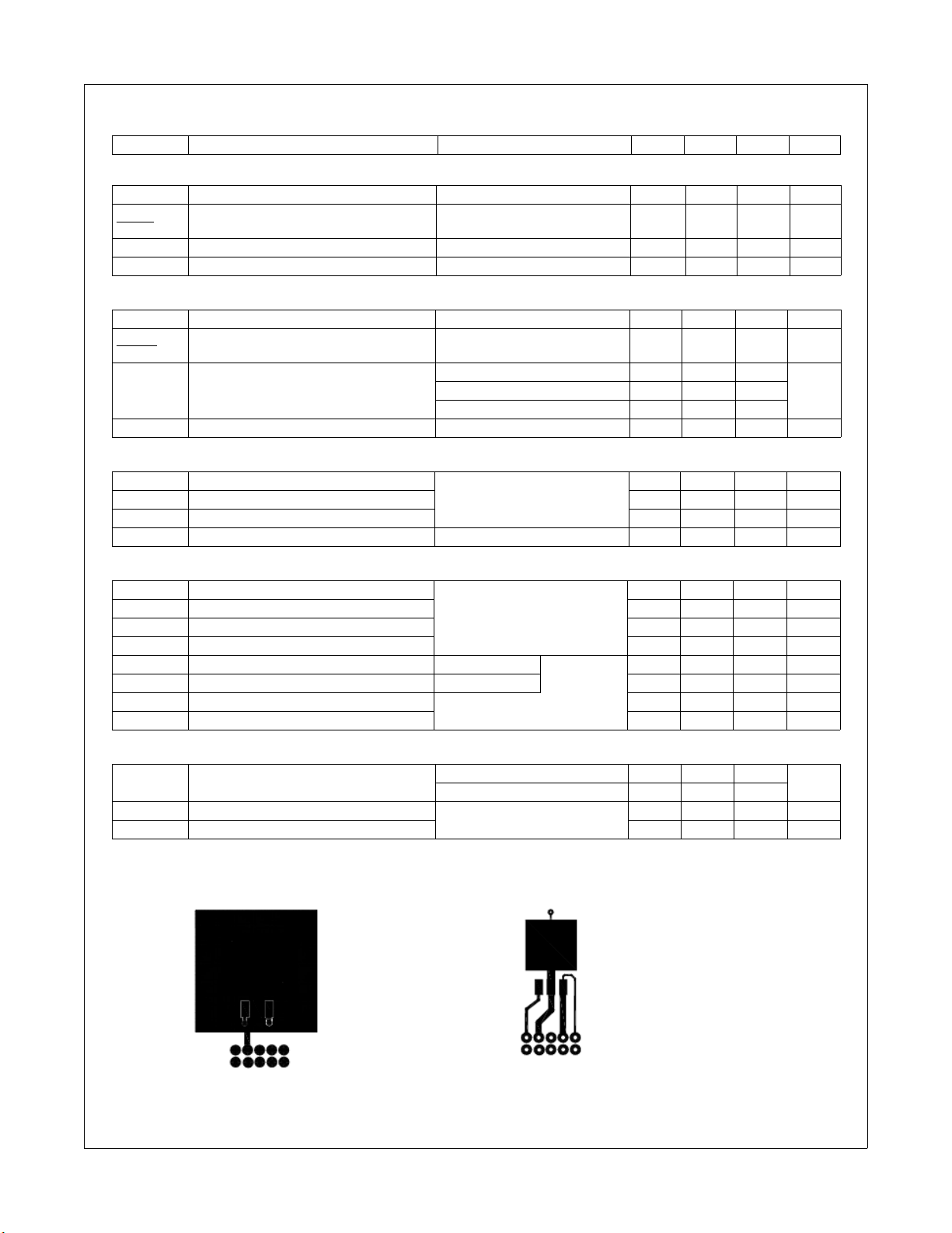
Package Marking and Ordering Information
A
W
°C/W
Device Marking Device Package Reel Size Tape Width Quantity
FDD6770A FDD6770A D-PAK (TO-252) 13 ’’ 12 mm 2500 units
©2009 Fairchild Semiconductor Corporation
FDD6770A Rev.C
1
www.fairchildsemi.com
FDD6770A N-Channel PowerTrench
Electrical Characteristics T
= 25 °C unless otherwise noted
J
Symbol Parameter Test Conditions Min Typ Max Units
Off Characteristics
BV
∆BV
∆T
I
DSS
I
GSS
DSS
DSS
J
Drain to Source Breakdown Voltage ID = 250 µA, VGS = 0 V 25 V
Breakdown Voltage Temperature
Coefficient
Zero Gate Voltage Drain Current VDS = 20 V, V
Gate to Source Leakage Current VGS = ±20 V, V
I
= 250 µA, referenced to 25 °C 16 mV/°C
D
= 0 V 1 µA
GS
= 0 V ±100 nA
DS
On Characteristics
V
GS(th)
∆V
∆T
r
DS(on)
g
FS
GS(th)
J
Gate to Source Threshold Voltage VGS = VDS, ID = 250 µA 1.0 1.7 3.0 V
Gate to Source Threshold Voltage
Temperature Coefficient
Static Drain to Source On Resistance
I
= 250 µA, referenced to 25 °C -6 mV/°C
D
V
= 10 V, ID = 24 A 2.9 4.0
GS
= 4.5 V, ID = 18.4 A 5.9 8.0
GS
= 10 V, ID = 24 A, TJ = 150 °C 4.4 6.1
V
GS
Forward Transconductance VDS = 5 V, ID = 24 A 148 S
Dynamic Characteristics
C
iss
C
oss
C
rss
R
g
Input Capacitance
Output Capacitance 392 525 pF
Reverse Transfer Capacitance 354 535 pF
Gate Resistance 1.2 Ω
Switching Characteristics
t
d(on)
t
r
t
d(off)
t
f
Q
Q
Q
Q
g
g
gs
gd
Turn-On Delay Time
Rise Time 714ns
Turn-Off Delay Time 24 44 ns
Fall Time 510ns
Total Gate Charge VGS = 0 V to 10 V
Total Gate Charge VGS = 0 V to 5 V 18 26 nC
Gate to Source Charge 4.8 nC
Gate to Drain “Miller” Charge 7.4 nC
= 13 V, VGS = 0 V,
V
DS
f = 1 MHz
= 13 V, ID = 24 A,
V
DD
V
= 10 V, R
GS
GEN
= 6 Ω
V
DD
I
= 24 A
D
= 13 V,
1805 2405 pF
918ns
33 47 nC
mΩV
®
MOSFET
Drain-Source Diode Characteristics
V
SD
t
rr
Q
rr
Notes:
1: R
θJA
R
θJC
2: Pulse Test: Pulse Width < 300 µs, Duty cycle < 2.0%.
of 50 mJ is based on starting TJ = 25 °C, L = 1 mH, IAS = 10 A, VDD = 23 V, VGS = 10 V. 100% test at L = 0.1 mH, IAS = 24 A.
3: E
AS
©2009 Fairchild Semiconductor Corporation
FDD6770A Rev.C
Source to Drain Diode Forward Voltage
Reverse Recovery Time
Reverse Recovery Charge 4 10 nC
is the sum of the junction-to-case and case-to-ambient thermal resistance where the case thermal reference is defined as the solder mounting surface of the drain pins .
is guaranteed by design while R
is determined by the user’s board design.
θJA
a)
40 °C/W when mounted on a
1 in2 pad of 2 oz copper
V
= 0 V, IS = 3.1 A (Note 2) 0.7 1.2
GS
= 0 V, IS = 24 A (Note 2) 0.8 1.3
V
GS
= 24 A, di/dt = 100 A/µs
I
F
2
b)
16 28 ns
96 °C/W when mounted on
a minimum pad
V
www.fairchildsemi.com
 Loading...