


Fairchild FDD4141 service manual
tm
FDD4141
(
)
P-Channel PowerTrench® MOSFET
-40V, -50A, 12.3mΩ
Features
Max r
Max r
High performance trench technology for extremely low r
RoHS Compliant
= 12.3mΩ at VGS = -10V, ID = -12.7A
DS(on)
= 18.0mΩ at VGS = -4.5V, ID = -10.4A
DS(on)
DS(on)
General Description
This P-Channel MOSFET has been produced using Fairchild
Semiconductor’s proprietary PowerTrench
deliver low
superior performance benefit in the applications.
switching performance capability reducing power dissipation
losses in converter/inverter applications.
r
Applications
Inverter
Power Supplies
July 2007
®
technology to
and optimized Bvdss capability to offer
DS(on)
and optimized
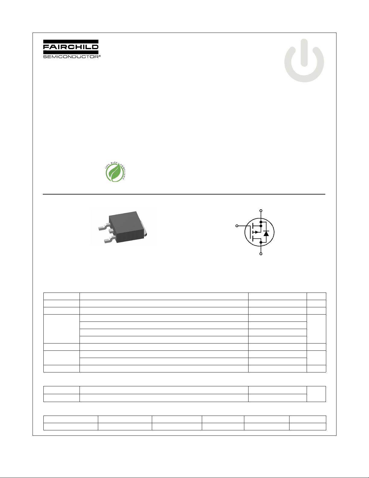
FDD4141 P-Channel PowerTrench
®
MOSFET
S
D
G
G
S
D-PAK
TO-252
TO-252
MOSFET Maximum Ratings T
Symbol Parameter Ratings Units
V
DS
V
GS
I
D
E
AS
P
D
, T
T
J
STG
Drain to Source Voltage -40 V
Gate to Source Voltage ±20 V
Drain Current -Continuous (Package limited) TC = 25°C -50
-Continuous (Silicon limited) T
-Continuous T
-Pulsed -100
Single Pulse Avalanche Energy (Note 3) 337 mJ
Power Dissipation TC = 25°C 69
Power Dissipation T
Operating and Storage Junction Temperature Range -55 to +150 °C
= 25°C unless otherwise noted
C
= 25°C -58
C
= 25°C (Note 1a) -10.8
A
= 25°C (Note 1a) 2.4
A
D
Thermal Characteristics
A
W
R
θJC
R
θJA
Thermal Resistance, Junction to Case 1.8
Thermal Resistance, Junction to Ambient (Note 1a) 52
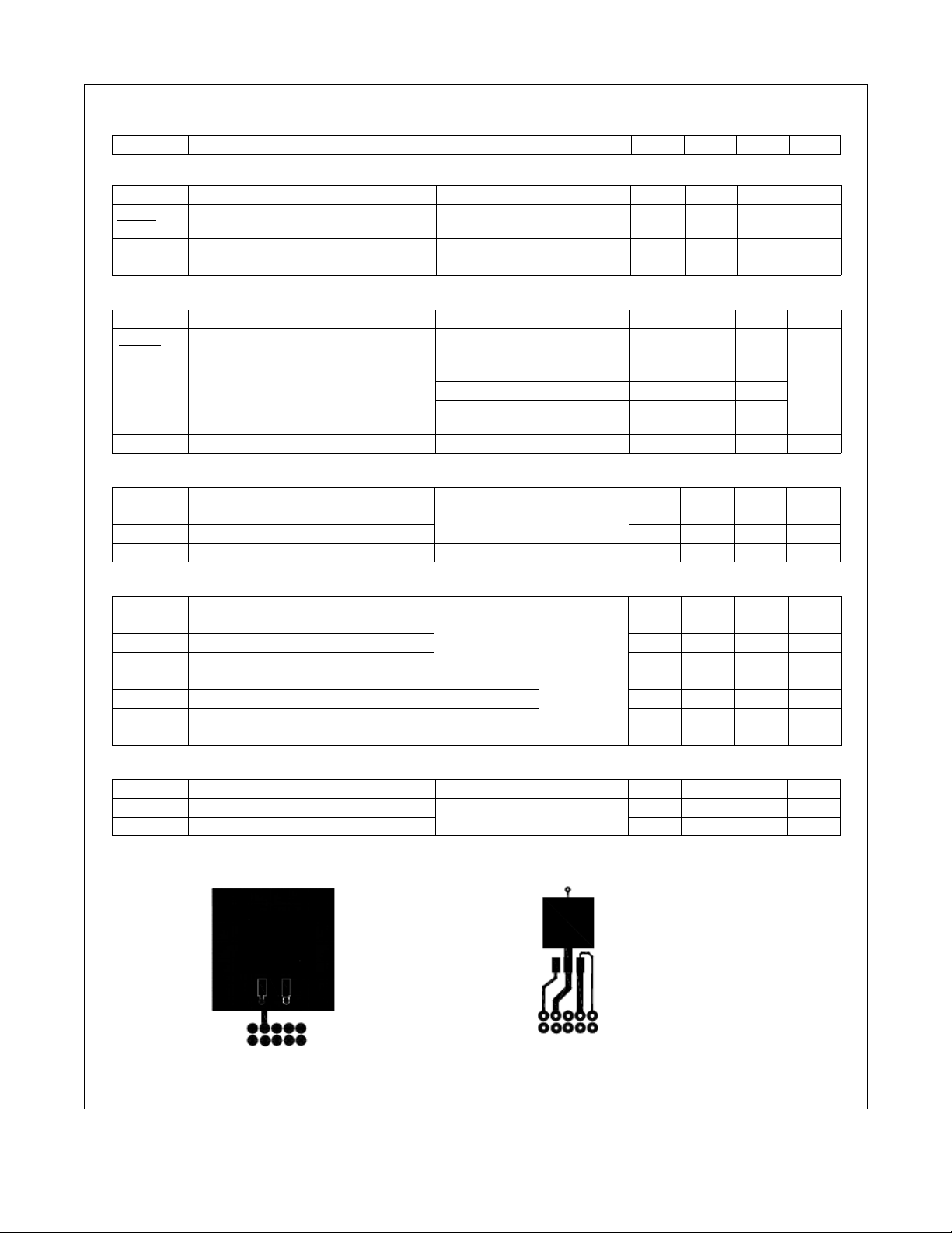
Package Marking and Ordering Information
Device Marking Device Package Reel Size Tape Width Quantity
FDD4141 FDD4141 D-PAK (TO-252) 13’’ 12mm 2500 units
©2007 Fairchild Semiconductor Corporation
FDD4141 Rev.C
°C/W
1
www.fairchildsemi.com
FDD4141 P-Channel PowerTrench
Electrical Characteristics T
= 25°C unless otherwise noted
J
Symbol Parameter Test Conditions Min Typ Max Units
Off Characteristics
BV
DSS
∆BV
DSS
∆T
J
I
DSS
I
GSS
On Characteristics
V
GS(th)
∆V
GS(th)
∆T
J
r
DS(on)
g
FS
Drain to Source Breakdown Voltage ID = -250µA, VGS = 0V -40 V
Breakdown Voltage Temperature
Coefficient
Zero Gate Voltage Drain Current VDS = -32V, V
Gate to Source Leakage Current VGS = ±20V, V
ID = -250µA, referenced to 25°C -29 mV/°C
= 0V -1 µA
GS
= 0V ±100 nA
DS
Gate to Source Threshold Voltage VGS = VDS, ID = -250µA -1 -1.8 -3 V
Gate to Source Threshold Voltage
Temperature Coefficient
Static Drain to Source On Resistance
Forward Transconductance VDS = -5V, ID = -12.7A 38 S
ID = -250µA, referenced to 25°C 5.8 mV/°C
VGS = -10V, ID = -12.7A 10.1 12.3
VGS = -4.5V, ID = -10.4A 14.5 18.0
VGS = -10V, ID = -12.7A,
TJ = 125°C
15.3 18.7
Dynamic Characteristics
C
iss
C
oss
C
rss
R
g
Input Capacitance
Output Capacitance 360 480 pF
Reverse Transfer Capacitance 210 310 pF
VDS = -20V, VGS = 0V,
f = 1MHz
2085 2775 pF
Gate Resistance f = 1MHz 4.6 Ω
mΩ
®
MOSFET
Switching Characteristics
t
d(on)
t
r
t
d(off)
t
f
Q
Q
Q
Q
g
g
gs
gd
Turn-On Delay Time
Rise Time 7 13 ns
Turn-Off Delay Time 38 60 ns
VDD = -20V, ID = -12.7A,
VGS = -10V, R
GEN
= 6Ω
10 19 ns
Fall Time 15 27 ns
Total Gate Charge V
Total Gate Charge V
Gate to Source Charge 7 nC
= 0V to -10V
GS
= 0V to -5V 19 27 nC
GS
VDD = -20V,
ID = -12.7A
36 50 nC
Gate to Drain “Miller” Charge 8 nC
Drain-Source Diode Characteristics
V
SD
t
rr
Q
rr
Notes:
1: R
R
θJA
θJC
Source to Drain Diode Forward Voltage V
Reverse Recovery Time
Reverse Recovery Charge 26 40 nC
is the sum of the junction-to-case and case-to-ambient thermal resistance where the case thermal reference is defined as the solder mounting surface of the drain pins.
is guaranteed by design while R
is determined by the user’s board design.
θJA
a)
52°C/W when mounted on a
2
pad of 2 oz copper
1 in
= 0V, IS = -12.7A (Note 2) -0.8 -1.2 V
GS
IF = -12.7A, di/dt = 100A/µs
29 44 ns
b)
100°C/W when mounted
on a minimum pad.
2: Pulse Test: Pulse Width < 300µs, Duty cycle < 2.0%.
3: Starting T
©2007 Fairchild Semiconductor Corporation
FDD4141 Rev.C
= 25°C, L = 3mH, IAS = 15A, VDD = 40V, VGS = 10V.
J
2
www.fairchildsemi.com