

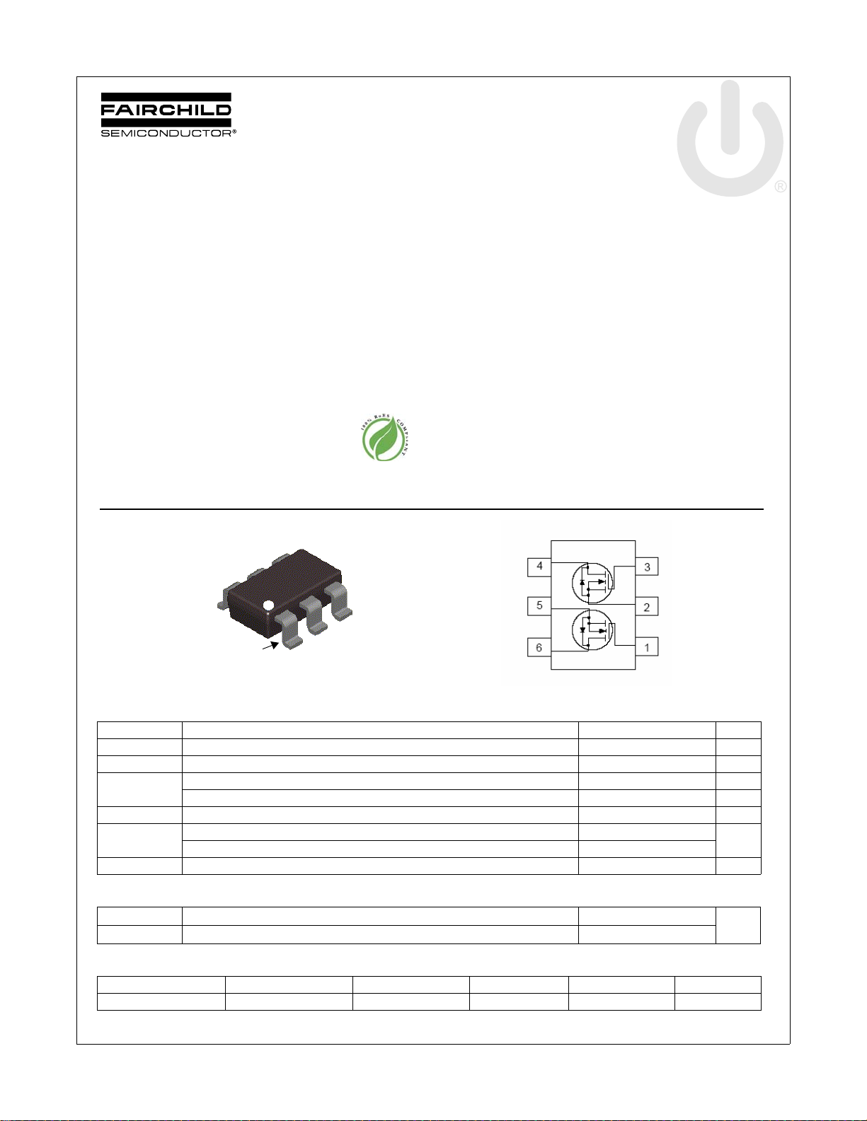
FDC8602
SuperSOTTM -6
G2
D2
S2
S1
D1
G1
Pin 1
Dual N-Channel PowerTrench® MOSFET
100 V, 1.2 A, 350 mΩ
Features
Max r
Max r
High performance trench technology for extremely low r
High power and current handling capability in a widely used
surface mount package
Fast switching speed
100% UIL Tested
RoHS Compliant
= 350 mΩ at VGS = 10 V, ID = 1.2 A
DS(on)
= 575 mΩ at VGS = 6 V, ID = 0.9 A
DS(on)
DS(on)
General Description
This N-Channel MOSFET is produced using Fairchild
Semiconductor‘s advanced Power Trench
been optimized for
ruggedness.
Applications
Load Switch
Synchronous Rectifier
®
process that has
r
, switching performance and
DS(on)
July 2011
FDC8602 Dual N-Channel PowerTrench
®
MOSFET
MOSFET Maximum Ratings T
Symbol Parameter Ratings Units
V
DS
V
GS
I
D
E
AS
P
D
, T
T
J
STG
Drain to Source Voltage 100 V
Gate to Source Voltage ±20 V
Drain Current -Continuous (Note 1a) 1.2 A
-Pulsed 5 A
Single Pulse Avalanche Energy (Note 3) 1.5 mJ
Power Dissipation (Note 1a) 0.96
Power Dissipation (Note 1b) 0.69
Operating and Storage Junction Temperature Range -55 to +150 °C
= 25 °C unless otherwise noted
A
W
Thermal Characteristics
R
θJC
R
θJA
Thermal Resistance, Junction to Case 60
Thermal Resistance, Junction to Ambient (Note 1a) 130
°C/W
Package Marking and Ordering Information
Device Marking Device Package Reel Size Tape Width Quantity
.862 FDC8602 SSOT-6 7 ’’ 8
©2011 Fairchild Semiconductor Corporation 1 www.fairchildsemi.com
FDC8602 Rev.C
mm 3000 units

FDC8602 Dual N-Channel PowerTrench
Electrical Characteristics T
= 25 °C unless otherwise noted
J
Symbol Parameter Test Conditions Min Typ Max Units
Off Characteristics
BV
ΔBV
ΔT
I
DSS
I
GSS
DSS
DSS
J
Drain to Source Breakdown Voltage I
Breakdown Voltage Temperature
Coefficient
Zero Gate Voltage Drain Current V
Gate to Source Leakage Current V
= 250 μA, VGS = 0 V 100 V
D
I
= 250 μA, referenced to 25 °C 73 mV/°C
D
= 80 V, V
DS
= ±20 V, V
GS
= 0 V1μA
GS
= 0 V ±100nA
DS
On Characteristics
V
GS(th)
ΔV
ΔT
r
DS(on)
g
FS
GS(th)
J
Gate to Source Threshold Voltage VGS = VDS, I
Gate to Source Threshold Voltage
Temperature Coefficient
Static Drain to Source On Resistance
Forward Transconductance V
I
= 250 μA, referenced to 25 °C -8 mV/°C
D
V
= 10 V, ID = 1.2 A 285 350
GS
= 6 V, ID = 0.9 A 409 575
GS
= 10 V, ID = 1.2 A, T
V
GS
= 10 V, ID = 1.2 A1.3S
DS
= 250 μA23.24V
D
= 125 °C 489 600
J
Dynamic Characteristics
C
iss
C
oss
C
rss
R
g
Input Capacitance
Output Capacitance 17 25 pF
Reverse Transfer Capacitance 0.8 5 pF
Gate Resistance 1.6 Ω
Switching Characteristics
t
d(on)
t
r
t
d(off)
t
f
Q
g(TOT)
Q
g(TOT)
Q
gs
Q
gd
Turn-On Delay Time
Rise Time 1.7 10 ns
Turn-Off Delay Time 5.4 11 ns
Fall Time 2.3 10 ns
Total Gate Charge V
Total Gate Charge V
Gate to Source Charge 0.4 nC
Gate to Drain “Miller” Charge 0.4 nC
= 50 V, VGS = 0 V,
V
DS
f = 1MHz
= 50 V, ID = 1.2 A,
V
DD
V
= 10 V, R
GS
= 0 V to 10 V
GS
= 0 V to 5 V0.61nC
GS
GEN
= 6 Ω
V
DD
I
= 1.2 A
D
= 50 V,
53 70 pF
3.5 10 ns
1.2 2 nC
mΩV
®
MOSFET
Drain-Source Diode Characteristics
V
SD
t
rr
Q
rr
NOTES:
1. R
is the sum of the junction-to-case and case -to-ambie nt ther mal resistan ce where the c ase ther mal referen ce is defi ned as the so lder moun ting su rface of the drai n pins.
θJA
R
is guaranteed by design while R
θJC
2. Pulse Test: Pulse Width < 300 μs, Duty cycle < 2.0%.
3. Starting T
©2011 Fairchild Semiconductor Corporation 2 www.fairchildsemi.com
FDC8602 Rev.C
Source-Drain Diode Forward Voltage V
Reverse Recovery Time
Reverse Recovery Charge 12 21 nC
is determined by the user's board design.
θCA
a)
130 °C/W when mounted on
a 1 in2 pad of 2 oz copper
= 25 °C; N-ch: L = 3 mH, IAS = 1 A, VDD = 100 V, VGS = 10 V.
J
= 0 V, IS = 1.2 A (Note 2) 0.86 1.3 V
GS
= 1.2 A, di/dt = 100 A/μs
I
F
27 43 ns
b)
180 °C/W when mounted on a
mi n im u m p ad o f 2 o z co ppe r
FDC8602 Dual N-Channel PowerTrench
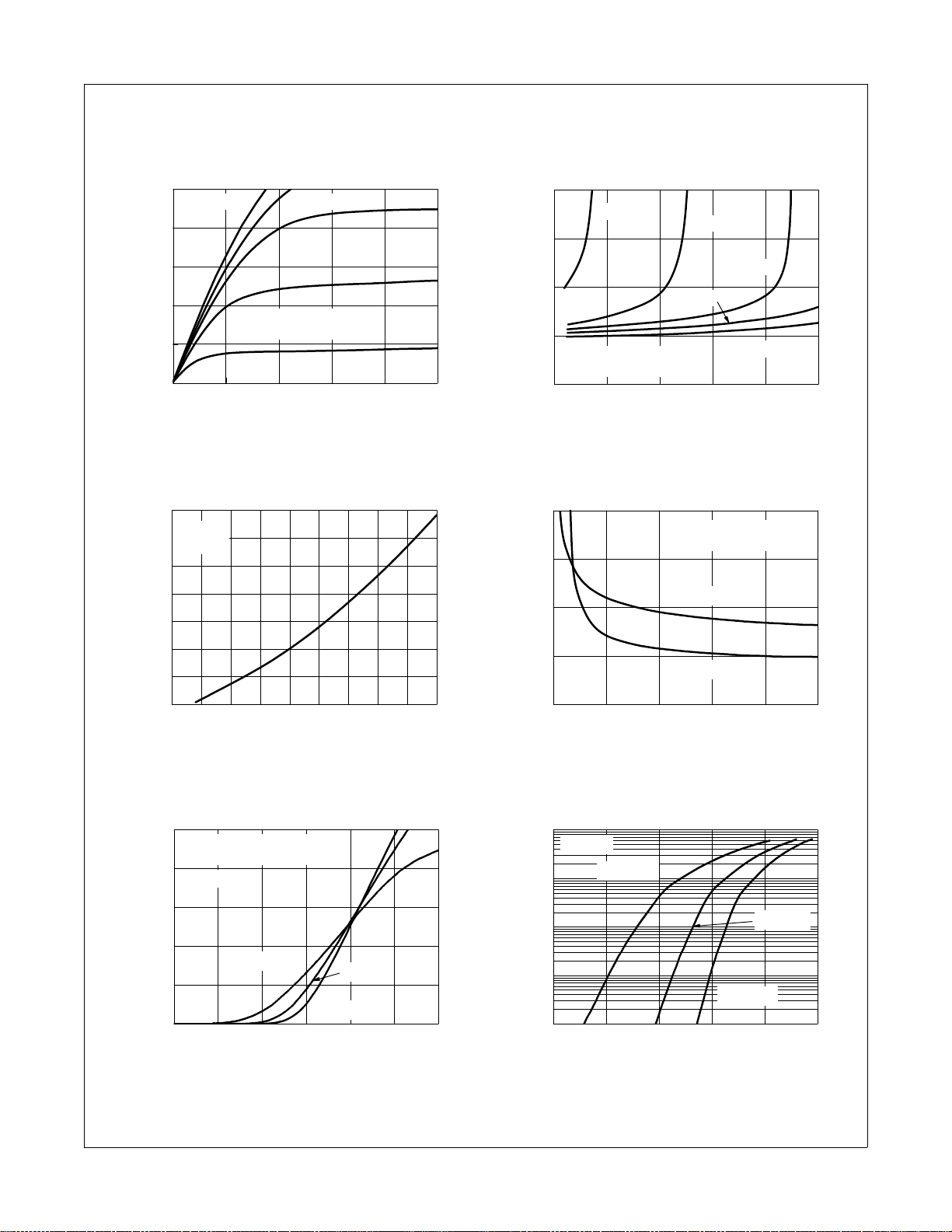
012345
0
1
2
3
4
5
VGS = 8 V
VGS = 7 V
V
DS
, DRAIN TO SOURCE VOLTAGE (V)
I
D
, DRAIN CURRENT (A)
VGS = 6 V
VGS = 5 V
VGS = 10 V
PULSE DURATION = 80 μs
DUTY CYCLE = 0.5% MAX
012345
0
1
2
3
4
VGS = 10 V
VGS = 5 V
VGS = 6 V
PULSE DURATION = 80 μs
DUTY CYCLE = 0.5% MAX
NORMALIZED
DRAIN TO SOURCE ON-RESISTANCE
I
D
, DRAIN CURRENT (A)
VGS = 7 V
VGS = 8 V
-75 -50 -25 0 25 50 75 100 125 150
0.6
0.8
1.0
1.2
1.4
1.6
1.8
2.0
ID = 1.2 A
V
GS
= 10 V
NORMALIZED
DRAIN TO SOURCE ON-RESISTANC E
T
J
, JUNCTION TEMPERATURE (
o
C)
5678910
0
300
600
900
1200
PULSE DURATION = 80 μs
DUTY CYCLE = 0.5% MAX
TJ = 125 oC
T
J
= 25
o
C
ID = 1.2 A
r
DS(on)
, DRAIN TO
SOURCE ON-RESISTANCE
(mΩ)
VGS, GATE TO SOURCE VO L TAGE (V)
2345678
0
1
2
3
4
5
TJ = 150 oC
V
DS
= 5 V
PULSE DURATION = 80 μs
DUTY CYCLE = 0.5% MAX
TJ = -55 oC
TJ = 25 oC
I
D
, DRAIN CURRENT (A)
VGS, GATE TO SOURCE VOLTAGE (V)
0.2 0.4 0.6 0.8 1.0 1.2
0.001
0.01
0.1
1
10
TJ = -55 oC
TJ = 25 oC
TJ = 150 oC
V
GS
= 0 V
I
S
, REVERSE DRAIN CURRENT (A)
VSD, BODY DIODE FORWARD VOLTAGE (V)
Typical Characteristics T
Figure 1.
On Region Characteristics Figure 2.
= 25 °C unless otherwise noted
J
Nor m aliz e d On- R esis t ance
vs Drain Current and Gate Voltage
®
MOSFET
Fi gure 3. Normali zed On Resi sta nce
vs Junction Temperature
©2011 Fairchild Semiconductor Corporation 3 www.fairchildsemi.com
FDC8602 Rev.C
Figure 5. Transfer Characteristics
Figure 4.
On-Resistance vs Gate to
Source Voltage
Figure 6.
Source to Drain Diode
Forward Voltage vs Source Current

FDC8602 Dual N-Channel PowerTrench
0 0.2 0.4 0.6 0.8 1.0 1.2 1.4
0
2
4
6
8
10
ID = 1.2 A
VDD = 75 V
V
DD
= 25 V
V
GS
, GATE TO SOURCE VOLTAGE (V)
Qg, GATE CHARGE (nC)
VDD = 50 V
0.1 1 10 100
0.1
1
10
500
f = 1 MHz
V
GS
= 0 V
CAPACITANCE (pF)
VDS, DRAIN TO SOURCE VOLTAGE (V)
C
rss
C
oss
C
iss
0.01 0.1 1 10
0.1
1
2
TJ = 100 oC
TJ = 25 oC
TJ = 125 oC
tAV, TIME IN AVALANCHE (ms)
I
AS
, AVALANCHE CURRENT (A)
0.1 1 10 100 400
0.005
0.01
0.1
1
10
100 us
1 ms
1 s
10 ms
DC
10 s
100 ms
I
D
, DRAIN CURRENT (A)
VDS, DRAIN to SOURCE VOLTAGE (V)
THIS A REA IS
LIMITED BY r
DS(on)
SINGLE PULSE
T
J
= MAX RATED
R
θJA
= 180
o
C/W
T
A
= 25
o
C
10
-4
10
-3
10
-2
10
-1
110
100 1000
0.5
1
10
100
VGS = 10 V
P
(PK)
, PEAK TRANSIENT POWER (W)
SINGLE PULSE
R
θJA
= 180 oC/W
T
A
= 25 oC
t, PULSE WIDTH (sec)
Typical Characteristics T
Figure 7.
Gate Charge Characteristics Figure 8.
= 25 °C unless otherwise noted
J
Capa c i tance v s Drai n
to Source Voltage
®
MOSFET
Figure 9.
Unclam p e d I nductiv e
Switching Capability
©2011 Fairchild Semiconductor Corporation 4 www.fairchildsemi.com
FDC8602 Rev.C
Figure 10.
Operating Area
Figure 11. Single Pulse Maximum Power Dissipation
Forward Bias Safe

FDC8602 Dual N-Channel PowerTrench
10
-4
10
-3
10
-2
10
-1
110
100 1000
0.005
0.01
0.1
1
SINGLE PULSE
R
θJA
= 180 oC/W
DUTY CYCLE-DESCENDING ORDER
NORMALIZED THERMAL
IMPEDANCE,
Z
θJA
t, RECTANGULAR PULSE DURATION (sec)
D = 0.5
0.2
0.1
0.05
0.02
0.01
2
P
DM
t
1
t
2
NOTES:
DUTY FACTOR: D = t1/t
2
PEAK TJ = PDM x Z
θJA
x R
θJA
+ T
A
Typical Characteristics T
Figure 12.
= 25 °C unless otherwise noted
J
Junction-to-Ambient Transient Thermal Response Curve
®
MOSFET
©2011 Fairchild Semiconductor Corporation 5 www.fairchildsemi.com
FDC8602 Rev.C

FDC8602 Dual N-Channel PowerTrench
Dimensional Outline and Pad Layout
®
MOSFET
©2011 Fairchild Semiconductor Corporation 6 www.fairchildsemi.com
FDC8602 Rev.C

TRADEMARKS
tm
®
tm
™
tm
The following includes registered and unregistered trademarks and service marks, owned by Fairchild Semi conductor and/or its glob al subsidiaries, and is not
intended to be an exhaustive list of all such trademarks.
2Cool™
AccuPower™
Auto-SPM™
AX-CAP™*
®
BitSiC
Build it Now™
CorePLUS™
CorePOWER™
CROSSVOLT™
CTL™
Current Transfer Logic™
DEUXPEED
Dual Cool™
EcoSPARK
EfficentMax™
®
®
ESBC™
®
Fairchild
Fairchild Semiconductor
FACT Quiet Series™
®
FACT
®
FAST
FastvCore™
FETBench™
®
FlashWriter
FPS™
F-PFS™
FRFET
Global Power Resource
Green FPS™
Green FPS™ e-Series™
Gmax™
GTO™
IntelliMAX™
ISOPLANAR™
MegaBuck™
MICROCOUPLER™
MicroFET™
MicroPak™
MicroPak2™
MillerDrive™
MotionMax™
Motion-SPM™
mWSaver™
OptiHiT™
OPTOLOGIC
OPTOPLANAR
®
*
®
®
®
®
PDP SPM™
Power-SPM™
PowerTrench
PowerXS™
SM
Programmable Active Droop™
QFET
QS™
Quiet Series™
RapidConfigure™
®
®
Saving our world, 1mW/W/kW at a time™
SignalWise™
SmartMax™
SMART START™
®
SPM
STEALTH™
SuperFET
SuperSOT™-3
SuperSOT™-6
SuperSOT™-8
SupreMOS
SyncFET™
Sync-Lock™
®
®
®*
The Power Franchise
The Right Technology for Y our Success™
TinyBoost™
TinyBuck™
TinyCalc™
®
TinyLogic
TINYOPTO™
TinyPower™
TinyPWM™
TinyWire™
®
TranSiC
TriFault Detect™
TRUECURRENT
μSerDes™
®
UHC
Ultra FRFET™
UniFET™
VCX™
VisualMax™
XS™
®
®
®
*
FDC8602 Dual N-Channel PowerTrench
®
MOSFET
*Trademarks of System General Corporation, used under license by Fairchild Semiconductor.
DISCLAIMER
FAIRCHILD SEMICONDUCTOR RESERVES THE RIGHT TO MAKE CHANGES WITHOUT FURTHER NOTICE TO ANY PRODUCTS HEREIN TO IMPROVE
RELIABILITY, FUNCTION, OR DESIGN. FAIRCHILD DOES NOT ASSUME ANY LIABILITY ARISING OUT OF THE APPLICATION OR USE OF ANY
PRODUCT OR CIRCUIT DESCRIBED HEREIN; NEITHER DOES IT CONVEY ANY LICENSE UNDER ITS PATENT RIGHTS, NOR THE RIGHTS OF OTHERS.
THESE SPECIFICATIONS DO NOT EXPAND THE TERMS OF FAIRCHILD’S WORLDWIDE TERMS AND CONDITIONS, SPECIFICALLY THE WARRANTY
THEREIN, WHICH COVERS THESE PRODUCTS.
LIFE SUPPORT POLICY
FAIRCHILD’S PRODUCTS ARE NOT AUTHORIZED FOR USE AS CRITICAL COMPONENTS IN LIFE SUPPORT DEVICES OR SYSTEMS WITHOUT THE
EXPRESS WRITTEN APPROVAL OF FAIRCHILD SEMICONDUCTOR CORPORATION.
As used here in:
1. Life support devices or systems are devices or systems which, (a) are
intended for surgical implant into the body or (b) support or sustain life,
and (c) whose failure to perform when properly used in accordance with
instructions for use provided in the labeling, can be reasonably
expected to result in a significant injury of the user.
ANTI-COUNTERFEITING POLICY
Fairchild Semiconductor Corporation’s Anti-Counterfeiting Policy. Fairchild’s Anti-Counterfeiting Policy is also stated on our external website,
www.Fairchildsemi.com, under Sales Support
Counterfeiting of semiconductor parts is a growing problem in the industry. All ma nufactures of semiconductor products are exper iencing counterfeiting of their
parts. Customers who inadvertently purchase counterfeit parts experience many proble ms su ch as loss of brand repu tation , substa ndard pe rfo rmance, f aile d
application, and increased cost of production and manufacturing delays. Fairchild is takin g stron g measures to protect ourselves and our customers from th e
proliferation of counterfeit parts. Fairchild str ongly encourages customers t o purchase Fairchild par ts either d irectly from Fairchild o r from Authorized Fairchild
Distributors who are listed by country on our web page cited above. Products customers buy either from Fairchild directly or from Authorized Fairchild
Distributors are genuine parts, have full traceability, meet Fairchild’s quality standards for handing and storage and provide access to Fairchild’s full range of
up-to-date technical and product information. Fairchild and our Authorized Distributors will stand behind all warranties and will appropriately address and
warranty issues that may arise. Fairchild will not provide any warranty coverage or other assistance for parts bought from Unauthorized Sources. Fairchild is
committed to combat this global problem and encourage our customers to do their part in stopping t his practice by buying direct or from authorized distributor s.
PRODUCT STATUS DEFINITIONS
Definition of Terms
.
2. A critical component in any component of a life support, device, or
system whose failure to perform can be reasonably expected to ca use
the failure of the life support device or system, or to affect its safety or
effectiveness.
Datasheet Identification Product Status Definition
Advance Information Formative / In Design
Preliminary First Production
No Identification Needed Full Production
Obsolete Not In Production
Datasheet contains the design specifications fo r product development. Specifications
may change in any manner without notice.
Datasheet contains preliminary data; supplementary data will be published at a later
date. Fairchild Semiconductor reserves the right to make changes at any time without
notice to improve design.
Datasheet contains final specifications. Fairchild Semiconductor reserves the right to
make changes at any time without notice to improve the design.
Datasheet contains specifications on a product that is discontinued by Fairchild
Semiconductor. The datasheet is for reference information only.
Rev. I55
©2011 Fairchild Semiconductor Corporation 7 www.fairchildsemi.com
FDC8602 Rev.C
 Loading...