Fairchild FDC855N service manual

tm
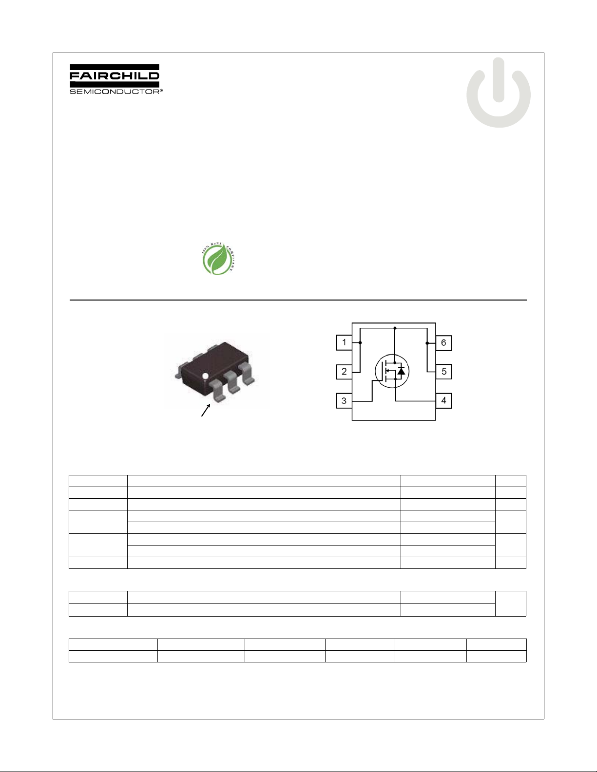
FDC855N
Single N-Channel, Logic Level, PowerTrench® MOSFET
30V, 6.1A, 27mΩ
Features
Max r
Max r
SuperSOTTM -6 package: small footprint (72% smaller than
standard SO-8; low profile (1mm thick).
RoHS Compliant
= 27mΩ at V
DS(on)
= 36mΩ at V
DS(on)
SuperSOT
TM
GS
GS
D
-6
= 10V, ID = 6.1A
= 4.5V, ID = 5.3A
S
D
G
D
D
General Description
This N-Channel Logic Level MOSFET is an efficient solution for
low voltage and battery powered applications. Utilizing Fairchild
Semiconductor’s advanced PowerTrench
possesses minimized on-state resistance to optimize the power
consumption. They are ideal for applications where in-line power
loss is critical.
Application
Power Management in Notebook, Hard Disk Drive
D
D
G
January 2008
®
process, this device
D
D
S
FDC855N N-Channel, Logic Level, PowerTrench
®
MOSFET
Pin 1
MOSFET Maximum Ratings T
Symbol Parameter Ratings Units
V
DS
V
GS
I
D
P
D
, T
T
J
STG
Drain to Source Voltage 30 V
Gate to Source Voltage ±20 V
Drain Current -Continuous TA = 25°C (Note 1a) 6.1
-Pulsed 20
Power Dissipation (Steady S t ate) (Note 1a) 1.6
Power Dissipation (Steady S t ate) (Note 1b) 0.8
Operating and Storage Junction Temperature Range -55 to +150 °C
= 25°C unless otherwise noted
A
Thermal Characteristics
R
θJC
R
θJA
Thermal Resistance, Junction to Case (Note 1) 30
Thermal Resistance, Junction to Ambient (Note 1a) 78
Package Marking and Ordering Information
Device Marking Device Package Reel Size Tape Width Quantity
.855 FDC855N SuperSOT-6 7” 8 mm 3000 units
A
W
°C/W
©2008 Fairchild Semiconductor Corporation
FDC855N Rev.C
1
www.fairchildsemi.com

Electrical Characteristics T
= 25°C unless otherwise noted
J
Symbol Parameter Test Conditions Min Typ Max Units
Off Characteristics
BV
∆BV
∆T
I
DSS
I
GSS
DSS
DSS
J
Drain to Source Breakdown Voltage ID = 250µA, VGS = 0V 30 V
Breakdown Voltage Temperature
Coefficient
Zero Gate Voltage Drain Current
Gate to Source Leakage Current VGS = ±20V, V
ID = 250µA, referenced to 25°C 24 mV/°C
V
= 0V, VDS = 24V, 1
GS
TC = 125°C 250
= 0V ±100 nA
DS
FDC855N N-Channel, Logic Level, PowerTrench
µA
On Characteristics
V
GS(th)
∆V
∆T
r
DS(on)
g
FS
GS(th)
J
Gate to Source Threshold Voltage VGS = VDS, ID = 250µA 1.0 2.0 3.0 V
Gate to Source Threshold Voltage
Temperature Coefficient
Static Drain to Source On Resistance
Forward Transconductance VDD = 10V, ID = 6.1A 20 S
Dynamic Characteristics
C
iss
C
oss
C
rss
R
g
Input Capacitance
Output Capacitance 108 145 pF
Reverse Transfer Capacitance 62 95 pF
Gate Resistance f = 1MHz 1.0 Ω
Switching Characteristics
t
d(on)
t
r
t
d(off)
t
f
Q
Q
Q
Q
g
g
gs
gd
Turn-On Delay Time
Rise Time 2 10 ns
Turn-Off Delay Time 14 23 ns
Fall Time 2 10 ns
Total Gate Charge at 10V VGS = 0V to 1 0 V
Total Gate Charge at 5V VGS = 0V to 5V 4.9 7.0 nC
Gate to Source Charge 1.7 nC
Gate to Drain “Miller” Charge 3.1 nC
ID = 250µA, referenced to 25°C -6 mV/°C
VGS = 10V, ID = 6.1A 20.7 27.0
mΩVGS = 4.5V, ID = 5.3A 28.2 36.0
VGS = 10V, ID = 6.1A, TJ =125°C 30.1 39.3
VDS = 15V, VGS = 0V,
493 655 pF
f = 1MHz
6 12 ns
VDD = 15V, ID = 6.1A,
VGS = 10V, R
GEN
= 6Ω
9.2 13 nC
VDD = 15V,
ID = 6.1A
®
MOSFET
Drain-Source Diode Characteristics
V
SD
t
rr
Q
rr
Notes:
1: R
θJA
is guaranteed by design while R
R
θJC
2: Pulse Test: Pulse Width < 300 µs, Duty Cycle < 2.0%.
©2008 Fairchild Semiconductor Corporation
FDC855N Rev.C
Source to Drain Diode Forward Voltage V
Reverse Recovery Time
Reverse Recovery Charge 6 12 nC
is the sum of the junction-to-case and ca se-to- a mbien t ther mal r esistance wher e the case the rmal refer ence i s defi ned as the solder m ount ing sur face of the dr ain pi ns.
is determined by the user’s board design.
θCA
= 0V, IS = 1.3A (Note 2) 0.80 1.2 V
GS
IF = 6.1A, di/dt = 100A/µs
a. 78°C/W when mounted on a
2
1 in
pad of 2 oz copper.
17 31 ns
b. 156°C/W when mounted on a
minimum pad of 2 oz copper.
2
www.fairchildsemi.com
 Loading...