

tm
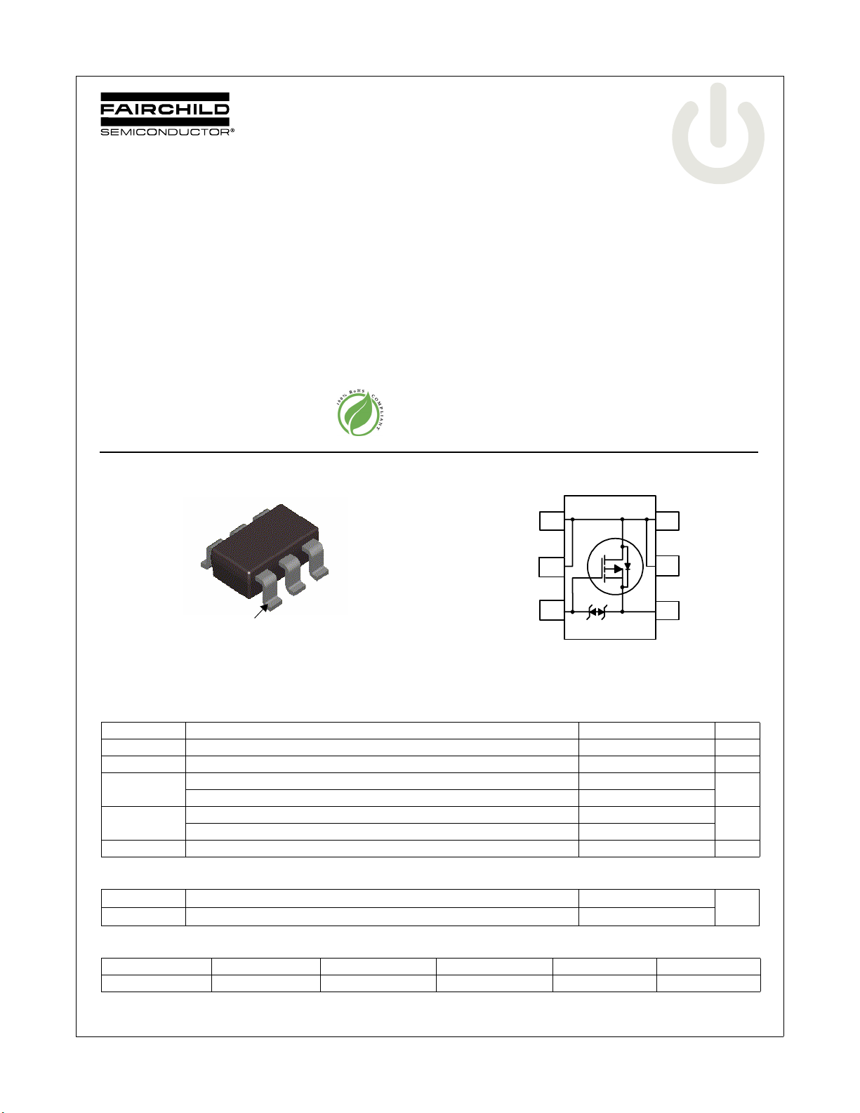
FDC610PZ
P-Channel PowerTrench® MOSFET
–30V, –4.9A, 42mΩ
Features
Max r
Max r
Low gate charge (17nC typical).
High performance trench technology for extremely low r
SuperSOTTM –6 package: small footprint (72% smaller than
standard SO–8) low profile (1mm thick).
RoHS Compliant
= 42mΩ at VGS = –10V, ID = –4.9A
DS(on)
= 75mΩ at VGS = –4.5V, ID = –3.7A
DS(on)
DS(on).
General Description
This P-Channel MOSFET is produced using Fairchild
Semiconductor’s advanced PowerTrench
been especially tailored to minimize the on-state resistance and
yet maintain low gate charge for superior switching performance.
These devices are well suited for battery power applications:
load switching and power management, battery charging
circuits, and DC/DC conversion.
Application
DC - DC Conversion
August 2007
®
process that has
FDC610PZ P-Channel PowerTrench
®
MOSFET
S
D
D
G
D
Pin 1
SuperSOTTM -6
MOSFET Maximum Ratings T
Symbol Parameter Ratings Units
V
DS
V
GS
I
D
P
D
, T
T
J
STG
Drain to Source Voltage –30 V
Gate to Source Voltage ±25 V
Drain Current -Continuous (Note 1a) –4.9
-Pulsed –20
Power Dissipation (Note 1a) 1.6
Power Dissipation (Note 1b) 0.8
Operating and Storage Junction Temperature Range –55 to +150 °C
D
= 25°C unless otherwise noted
A
D
1
D
2
G
3
3
D
6
D
5
S
4
Thermal Characteristics
R
θJA
R
θJA
Thermal Resistance, Junction to Ambient (Note 1a) 78
Thermal Resistance, Junction to Ambient (Note 1b) 156
Package Marking and Ordering Information
A
W
°C/W
Device Marking Device Package Reel Size Tape Width Quantity
.610Z FDC610PZ SSOT6 7’’ 8mm 3000units
©2007 Fairchild Semiconductor Corporation
FDC610PZ Rev.B
1
www.fairchildsemi.com
FDC610PZ P-Channel PowerTrench
Electrical Characteristics T
= 25°C unless otherwise noted
J
Symbol Parameter Test Conditions Min Typ Max Units
Off Characteristics
BV
DSS
∆BV
DSS
∆T
J
I
DSS
I
GSS
On Characteristics
V
GS(th)
∆V
GS(th)
∆T
J
r
DS(on)
g
FS
Drain to Source Breakdown Voltage ID = –250µA, VGS = 0V –30 V
Breakdown Voltage Temperature
Coefficient
Zero Gate Voltage Drain Current VDS = –24V, V
Gate to Source Leakage Current VGS = ±25V, V
ID = –250µA, referenced to 25°C –22 mV/°C
= 0V –1 µA
GS
= 0V ±10 µA
DS
Gate to Source Threshold Voltage VGS = VDS, ID = –250µA –1 –2.2 –3 V
Gate to Source Threshold Voltage
Temperature Coefficient
Static Drain to Source On Resistance
Forward Transconductance VDD = –10V, ID = –4.9A 15 S
ID = –250µA, referenced to 25°C 6 mV/°C
VGS = –10V, ID = –4.9A 36 42
VGS = –10V, ID = –4.9A, TJ = 125°C 50 60
Dynamic Characteristics
C
iss
C
oss
C
rss
R
g
Input Capacitance
Output Capacitance 145 195 pF
Reverse Transfer Capacitance 125 190 pF
VDS = –15V, VGS = 0V,
f = 1MHz
755 1005 pF
Gate Resistance f = 1MHz 13 Ω
Switching Characteristics
t
d(on)
t
r
t
d(off)
t
f
Q
Q
Q
Q
g
g
gs
gd
Turn-On Delay Time
Rise Time 4 10 ns
Turn-Off Delay Time 33 53 ns
VDD = –15V, ID = –4.9A
VGS = –10V, R
GEN
= 6Ω
7 14 ns
Fall Time 23 37 ns
Total Gate Charge V
Total Gate Charge V
Gate to Source Gate Charge 2.9 nC
= 0V to –10V
GS
= 0V to –4.5V 9 13 nC
GS
VDD = –15V,
17 24 nC
ID = –4.9A
Gate to Drain “Miller” Charge 4.3 nC
mΩVGS = –4.5V, ID = –3.7A 58 75
®
MOSFET
Drain-Source Diode Characteristics
I
S
V
SD
t
rr
Q
rr
Notes:
is determined with the device mounted on a 1in2 pad 2 oz copper pad on a 1.5 x 1.5 in. board of FR-4 material. R
1. R
θJA
the user's board design.
2. Pulse Test: Pulse Width < 300µs, Duty cycle < 2.0%.
FDC610PZ Rev.B
Maximum Continuous Drain-Source Diode Forward Current –1.3 A
Source to Drain Diode Forward Voltage V
Reverse Recovery Time
Reverse Recovery Charge 9 18 nC
= 0V, IS = –1.3A (Note 2) –0.8 –1.2 V
GS
IF = –4.9A, di/dt = 100A/µs
a. 78°C/W when mounted on a
2
1 in
pad of 2 oz copper.
19 35 ns
is guaranteed by design while R
θJC
b. 156°C/W when mounted on a
minimum pad of 2 oz copper.
2
is determined by
θCA
www.fairchildsemi.com
 Loading...