Fairchild FDP8880, FDB8880 service manual

0
May 2008
FDP8880 / FDB8880
FDP8880 / FDB 8880
N-Channel PowerTrench
30V, 54A, 11.6mΩ
Features
r
= 14.5mΩ, V
DS(ON)
r
= 11.6mΩ, V
DS(ON)
High pe rformance trench tech nology for e xtremely low
r
DS(ON)
Low gat e ch arge
High power and current handling capability
RoHS Complicant
= 4.5V, ID = 40A
GS
= 10V, ID = 40A
GS
®
MOSFET
General Description
This N- Channe l MOSF ET has been desig ned sp ecif icall y to
improve the overall efficiency of DC/DC converters using
either synchronous or conventional switching PWM
contro llers. It ha s be en optimize d for low gate cha r ge , low
r
and fast switching speed.
DS(ON)
Application
DC / DC Converters
tmM
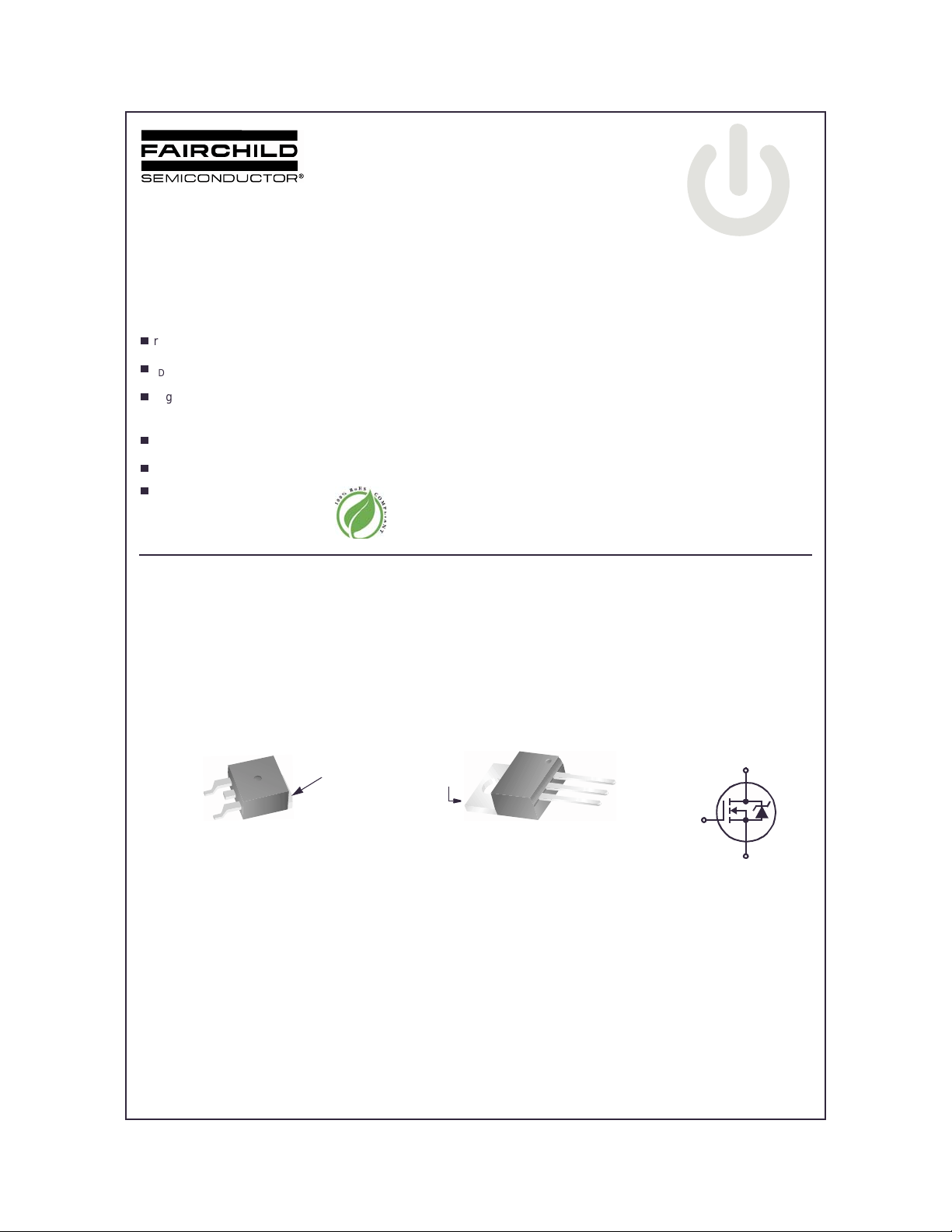
DRAIN
(FLANGE)
GATE
SOURCE
TO-263AB
FDB SERIES
©2008 Fairchild Semiconductor Corporation
FDP8880 / FDB8880 Rev. A1
(FLANGE)
DRAIN
1
TO-220AB
FDP SERIES
DRAIN
GATE
SOURCE
D
G
S
www.fairchildsemicom

FDP8880 / FDB8880
MOSFET Maximum Ratings T
= 25°C unless otherwise noted
C
Symbol Parameter Ratings Units
V
DSS
V
GS
Drain to Sou r c e Voltage 30 V
Gate to Source Voltage ±20 V
Drain Cur re nt
Continuous (T
I
D
Continuous (T
Continuous (T
= 25oC, VGS = 10V)
C
= 25oC, VGS = 4.5V) 48 A
C
= 25oC, VGS = 10V, with R
amb
= 43oC/W) 11 A
θJA
54 A
Pulsed Figure 4 A
E
AS
P
D
T
, T
J
STG
Single Pulse Avalanche Energy (Note 1) 31 mJ
Power dissipation 55 W
Derate above 25
o
C0.37W/
Operating and Storage Temperature -55 to 175
Thermal Characteristics
R
θJC
R
θJA
R
θJA
Thermal Resistance Junction to Case TO-220,TO-263 2.73
Thermal Resistance Junction to Am bient TO-220,TO-262 ( Note 2) 62
Thermal Resistance Junction to Am bient TO-263, 1in2 copper pad ar ea 43
Package Marking and Ordering Information
Device Marking Device Package Reel Size Tape Width Quantity
FDP8880 FDP8880 TO-220AB Tube N/A 50 units
FDB8880 FDB8880 TO-263AB 330mm 24mm 800 units
F
F
o
C/W
o
C/W
o
C/W
o
C
o
C
Electrical Characteristics
TC = 25°C unless otherwise noted
Symbol Parameter Test Condit ions Min Typ Max Units
Off Characteristics
B
I
DSS
I
GSS
VDSS
Drain to Sou r c e Br ea k down Voltage ID = 250µA, VGS = 0V 30 - - V
V
= 24V - - 1
Zero Gate Voltage Drain Current
DS
= 0V TC = 150oC- -250
V
GS
Gate to Source Leakage Current VGS = ±20V - - ±100 nA
On Characteristics
V
GS(TH)
r
DS(ON)
Gate to Source Threshold Vo ltage VGS = VDS, ID = 250µA 1.2 - 2.5 V
I
= 40A, VGS = 10V - 0.0095 0.011 6
D
= 40A, VGS = 4.5V - 0.012 0.0145
I
Drain to S ou r c e On Re si st ance
D
I
= 40A, VGS = 10V,
D
T
= 175oC
J
- 0.015 0.019
µA
Ω
©2008 Fairchild Semiconductor Corporation
DP8880 / FDB8880 Rev. A
F
1
2
www.fairchildsemicom

Dynamic Characteristics
C
C
C
R
Q
Q
Q
Q
Q
Q
ISS
OSS
RSS
G
g(TOT)
g(5)
g(TH)
gs
gs2
gd
Input Capacitance
Output Capacit ance - 255 - pF
Reverse Transfer Capacitance - 147 - pF
Gate Resistance VGS = 0.5V, f = 1MHz - 2.7 - Ω
Total Gate Charge at 10V VGS = 0V to 10V
Total Gate Charge at 5V VGS = 0V to 5V - 12 16 nC
Threshold Gate Charge VGS = 0V to 1V - 1.6 2.1 nC
Gate to Source Gate Charg e - 3.2 - nC
Gate Charge Threshold to Plateau - 2.0 - nC
Gate to Drain “Miller” Charge - 4.8 - nC
= 15V, VGS = 0V,
V
DS
f = 1MHz
V
DD
I
= 40A
D
= 1.0m A
I
g
FDP8880 / FDB8880
- 1240 - pF
-2229nC
= 15V
Switching Characteristics
t
ON
t
d(ON)
t
r
t
d(OFF)
t
f
t
OFF
Turn-On Time
Turn-On Delay Time - 8 - ns
Rise Time - 107 - ns
Turn-Off Delay Time - 47 - ns
Fall Time - 51 - ns
Turn-Off Time - - 147 ns
(VGS = 10V)
Drain-Source Diode Characteristics
V
SD
t
rr
Q
RR
Notes:
1: Starting TJ = 25°C, L = 34uH, IAS = 43A,Vdd = 27V, Vgs = 10V.
2: Pulse width = 100s.
3
Source to Drain Diode Voltage
Reverse Recovery Time ISD = 40A, dISD/dt = 100A/µs- -27ns
Reverse Recovered Charge ISD = 40A, dISD/dt = 100A/µs- -18nC
--171ns
= 15V, ID = 40A
V
DD
= 10V, RGS = 13.6Ω
V
GS
I
= 40A - - 1.25 V
SD
I
= 3.5A - - 1.0 V
SD
©2008 Fairchild Semiconductor Corporation
DP8880 / FDB8880 Rev. A
F
1
3
www.fairchildsemicom

FDP8880 / FDB8880
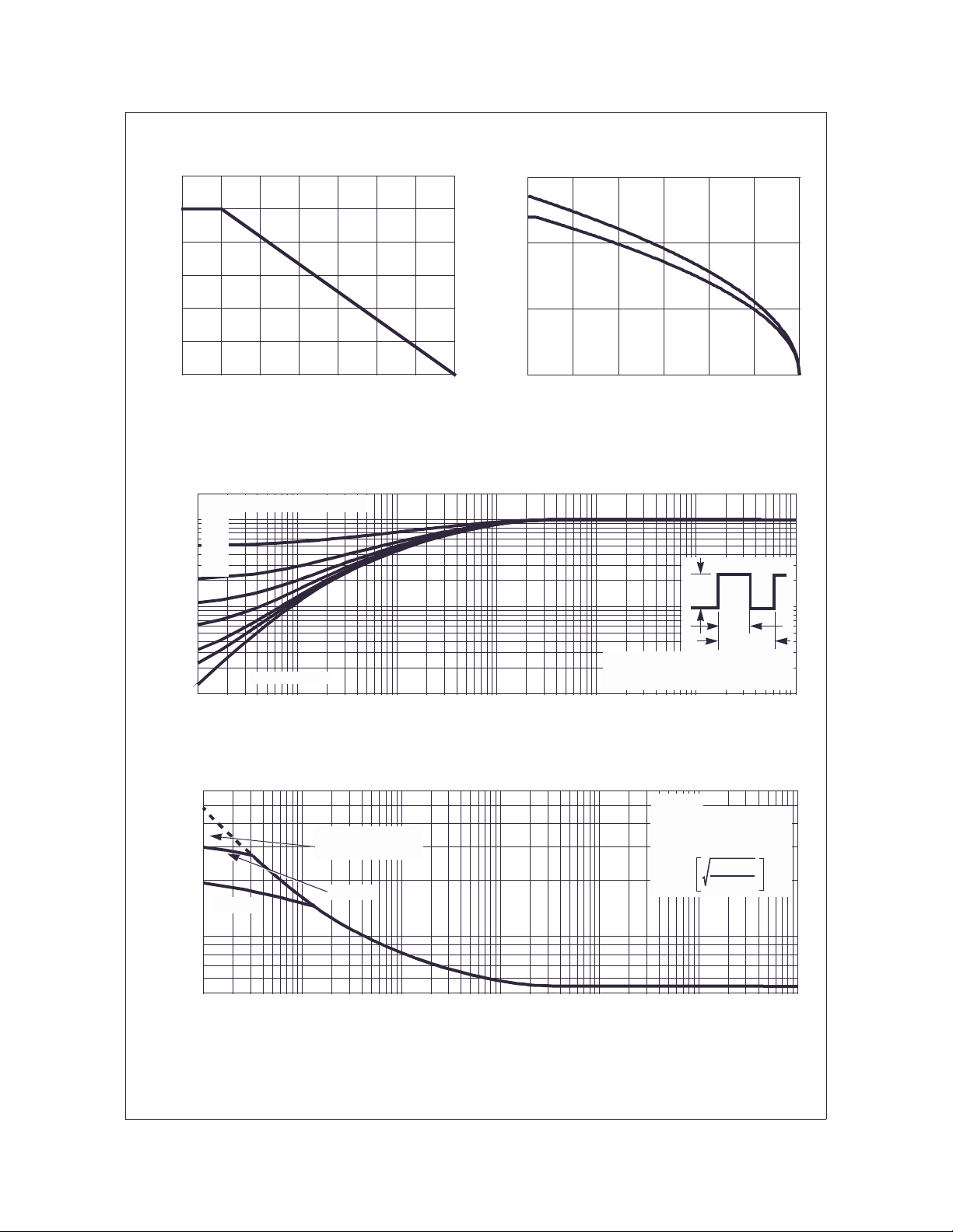
Typical Characteristics T
1.2
1.0
0.8
0.6
0.4
0.2
POWER DISSIPATION MULTIPLIER
0
0255075100 175
TC, CASE TEMPERATURE (oC)
= 25°C unless otherwise noted
C
150
125
Figure 1. Normalized Power Dissipation vs Case
Temperature
2
DUTY CYCLE - DESCENDING ORDER
0.5
1
0.2
0.1
0.05
0.02
0.01
0.1
, NORMALIZED
θJC
Z
THERMAL IMPEDANCE
0.01
-5
10
SINGLE PULSE
-4
10
-3
10
t, RECTANGULAR PULSE DURATION (s)
60
40
20
, DRAIN CURRENT (A)
D
I
0
25 50 75 100 125 150 175
TC, CASE TEMPERATURE (oC)
Figure 2. Maximum Continuous Drain Curr ent vs
Case Temperature
P
DM
t
1
t
x R
2
2
+ T
θJC
C
1
10
NOTES:
DUTY FACTOR: D = t1/t
PEAK TJ = PDM x Z
-2
10
-1
10
θJC
10
0
Figure 3. Normalized Maximum Transient Thermal Impedance
600
TRANSCONDUCTANCE
MAY LIMIT CURRENT
IN THIS REGION
VGS = 4.5V
, PEAK CURRENT (A)
100
DM
I
50
-5
10
©2008 Fairchild Semiconductor Corporation
F
DP8880 / FDB8880 Rev. A
-4
10
1
VGS = 10V
-3
10
-2
10
t, PULSE WIDTH (s)
Figure 4. Peak Current Capability
4
TC = 25oC
FOR TEMPERATURES
ABOVE 25oC DERATE PEAK
CURRENT AS FOLLOWS:
I = I
-1
10
175 - T
25
150
0
10
C
1
10
www.fairchildsemicom
 Loading...