tm
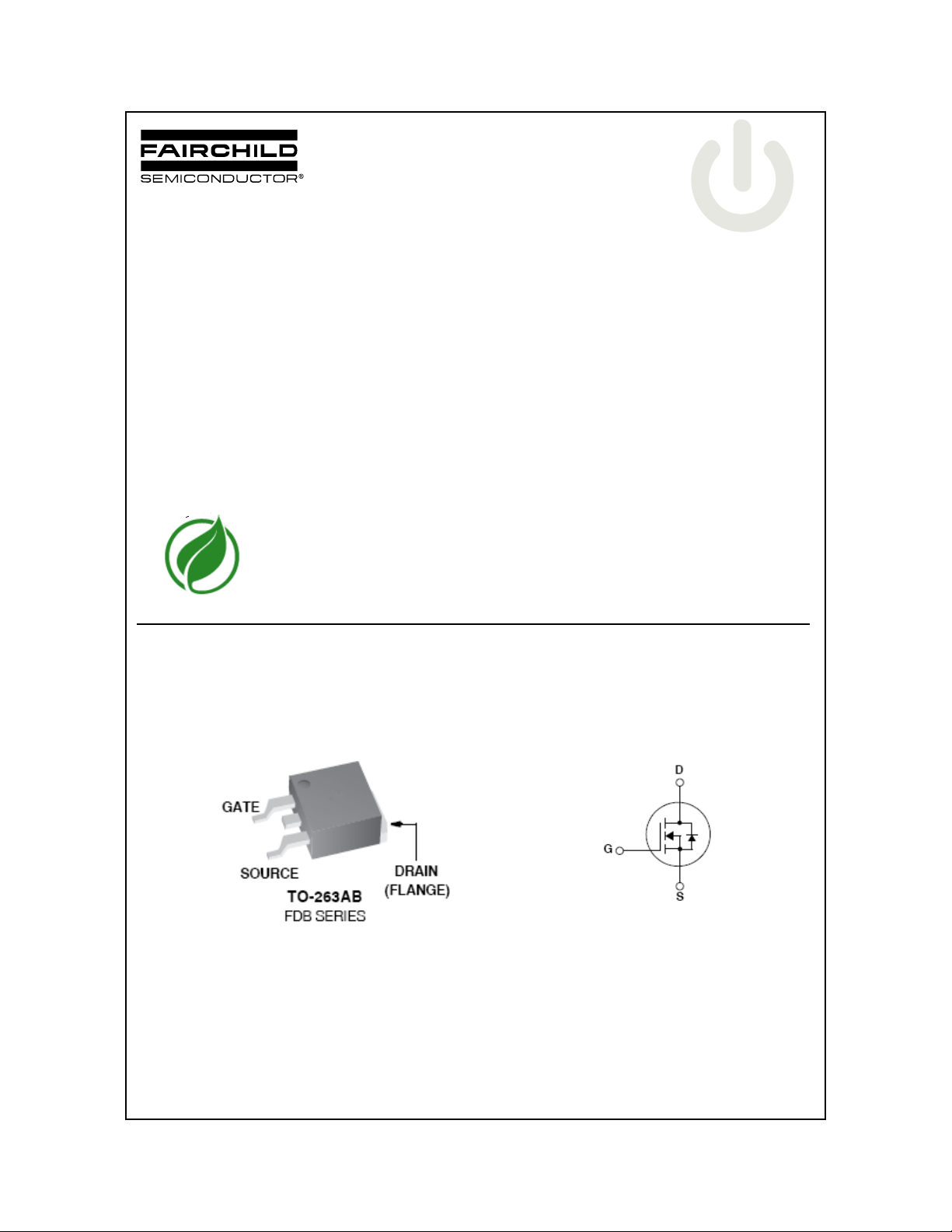
FDB8443
N-Channel PowerTrench® MOSFET
40V, 182A, 3.0mΩ
Features
Typ r
Typ Q
Low Miller Charge
Low Qrr Body Diode
UIS Capability (Single Pulse and Repetitive Pulse)
RoHS Compliant
= 2.3mΩ at V
DS(on)
= 142nC at VGS = 10V
g(10)
E
E
R
F
I
D
A
E
L
M
P
L
E
M
T
I
O
N
= 10V, ID = 80A
GS
E
N
T
A
June 2011
Applications
Power Tools
Automotive Engine Control
Powertrain Management
Solenoid and Motor Drivers
Electronic Steering
Integrated Starter / Alternator
Distributed Power Architecture and VRMs
Primary Switch for 12V Systems
FDB8443 N-Channel PowerTrench
®
MOSFET
©2011 Fairchild Semiconductor Corporation
FDB8443 Rev. A2
www.fairchildsemi.com1

FDB8443 N-Channel PowerTrench
MOSFET Maximum Ratings T
= 25°C unless otherwise noted
C
Symbol Parameter Ratings Units
V
DSS
V
GS
I
D
I
DM
E
AS
P
D
T
J
Drain to Source Voltage 40 V
Gate to Source Voltage ±20 V
= 25oC, Silicon Limited) 182*
C
= 100oC, Silicon Limited) 129*
C
= 25oC, Package Limited) 120
C
= 25oC, R
A
= 43oC/W) 25
θJA
Drain Current
- Continuous (T
- Continuous (T
- Continuous (T
- Continuous (T
D ra i n C u rr e n t - P u ls e d S ee Fi g u re 4
Single Pulse Avalanche Energy (Note 1) 531 mJ
Power Dissipation 188 W
o
Derate above 25
, T
Operating and Storage Temperature -55 to +175
STG
C1.25W/
*Calculated continuous current based on maximum allowable junction temperature. Package limitation current is 120A.
Thermal Characteristics
R
θJC
R
θJA
R
θJA
Thermal Resistance Junction to Case 0.8
Thermal Resistance Junction to Ambient (Note 2) 62
Thermal Resistance Junction to Ambient TO-263, 1in2 copper pad area 43
o
o
o
Package Marking and Ordering Information
Device Marking Device Package Reel Size Tape Width Quantity
FDB8443 FDB8443 TO-263AB 330mm 24mm 800 units
A
o
o
C
C/W
C/W
C/W
C
®
MOSFET
Electrical Characteristics T
= 25°C unless otherwise noted
C
Symbol Parameter Test Conditions Min Typ Max Units
Off Characteristics
B
I
DSS
I
GSS
VDSS
Drain to Source Breakdown Voltage ID = 250μA, VGS = 0V 40 - - V
V
= 32V, - - 1
Zero Gate Voltage Drain Current
DS
= 0V TC = 150oC - - 250
V
GS
Gate to Source Leakage Current VGS = ±20V - - ±100 nA
On Characteristics
V
GS(th)
r
DS(on)
Gate to Source Threshold Voltage VGS = VDS, ID = 250μA22.84V
= 80A, VGS= 10V - 2.3 3.0
I
Drain to Source On Resistance
D
I
= 80A, VGS= 10V,
D
T
= 175oC
J
-4.25.5
Dynamic Characteristics
C
iss
C
oss
C
rss
R
G
Q
Q
Q
Q
Q
g(TOT)
g(TH)
gs
gs2
gd
Input Capacitance
Output Capacitance - 800 - pF
Reverse Transfer Capacitance - 510 - pF
= 25V, VGS = 0V,
V
DS
f = 1MHz
Gate Resistance VGS = 0.5V, f = 1MHz - 0.9 - Ω
Total Gate Charge at 10V VGS = 0 to 10V
Threshold Gate Charge VGS = 0 to 2V - 17.5 23 nC
Gate to Source Gate Charge
Gate Charge Threshold to Plateau - 18.8 - nC
V
= 20V
DD
I
= 35A
D
I
= 1mA
g
Gate to Drain “Miller“ Charge - 32 - nC
- 9310 - pF
- 142 185 nC
-36-nC
μA
mΩ
FDB8443 Rev. A2 www.fairchildsemi.com2

FDB8443 N-Channel PowerTrench
Electrical Characteristics T
= 25oC unless otherwise noted
C
Symbol Parameter Test Conditions Min Typ Max Units
Switching Characteristics (V
t
on
t
d(on)
t
r
t
d(off)
t
f
t
off
Turn-On Time
Turn-On Delay Time - 18.4 - ns
Rise Time - 17.9 - ns
Turn-Off Delay Tim e - 55 - ns
Fall Time - 13.5 - ns
Turn-Off Time - - 109 ns
= 10V)
GS
= 20V, ID = 35A
V
DD
V
= 10V, RGS = 2Ω
GS
- - 58 ns
Drain-Source Diode Characteristics
I
= 35A - 0.8 1.25
V
SD
t
rr
Q
rr
Notes:
1: Starting TJ = 25oC, L = 0.26mH, IAS = 64A.
2: Pulse width = 100s.
Source to Drain Diode Voltage
Reverse Recovery Time
Reverse Recovery Charge - 48 62 nC
SD
= 15A - 0.8 1.0
I
SD
= 35A, dISD/dt = 100A/μs
I
SD
-4255ns
V
®
MOSFET
FDB8443 Rev. A2 www.fairchildsemi.com3
 Loading...