September 2005
FDB5800
N-Channel Logic Level PowerTrench® MOSFET
60V, 80A, 7mΩ
FDB5800 N-Channel Logic Level PowerTrench
Features
r
High performance trench technology for extermely low
Low Gate Charge
High power and current handling capability
Qualified to AEC Q101
RoHS Compliant
= 5.5mΩ (Typ.), V
DS(ON)
Rdson
= 5V, ID = 80A
GS
Applications
Motor/ Body Load Control
ABS Systems
Power Train Management
Injection Systems
DC-DC Converters and Off-Line UPS
®
MOSFET
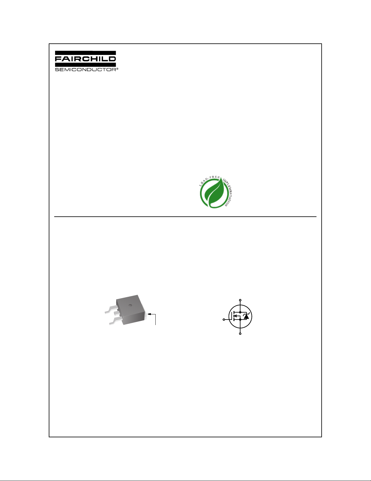
GATE
SOURCE
TO-263AB
FDB SERIES
©2005 Fairchild Semiconductor Corporation
FDB5800 Rev. A
DRAIN
(FLANGE)
D
G
S
www.fairchildsemi.com1

FDB5800 N-Channel Logic Level PowerTrench
MOSFET Maximum Ratings T
= 25°C unless otherwise noted
C
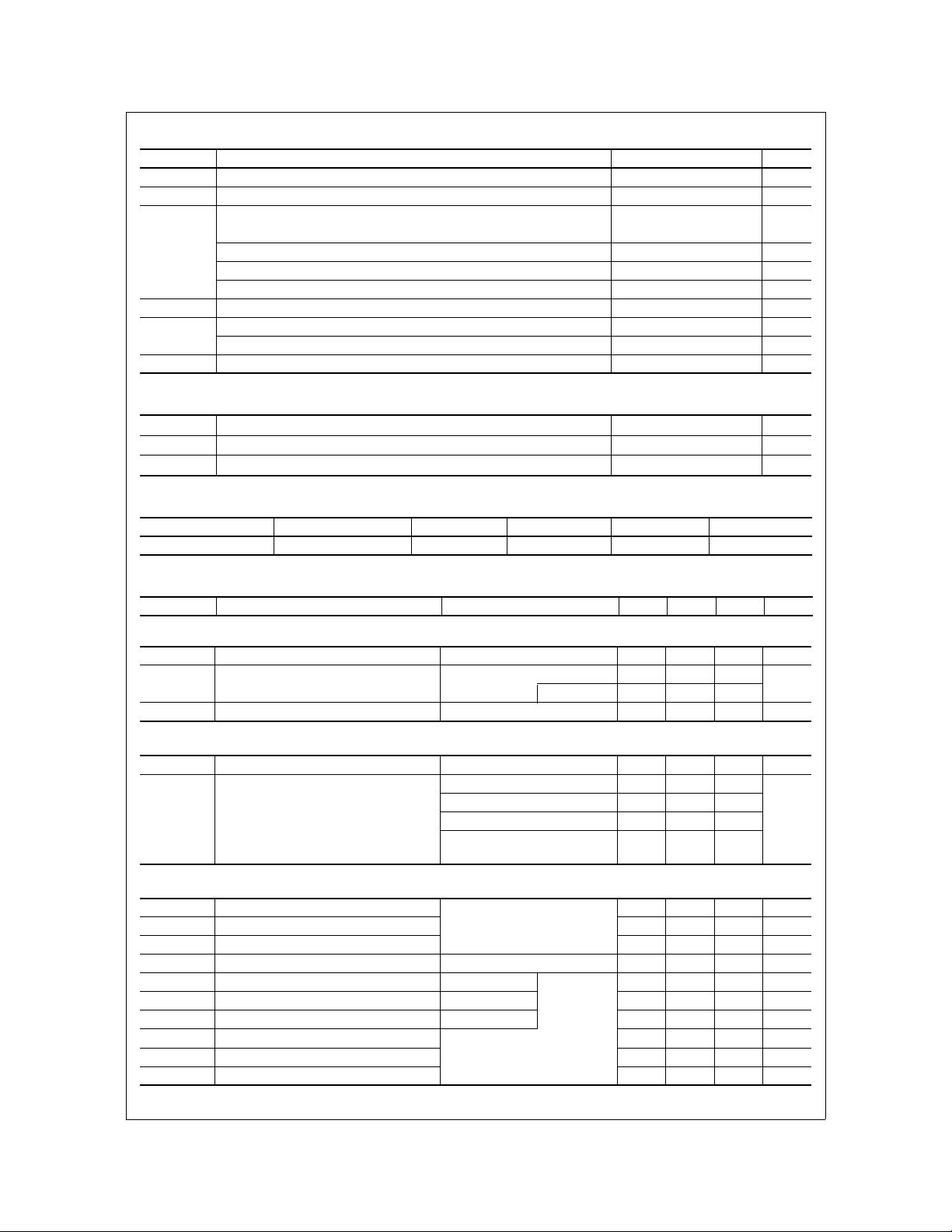
Symbol Parameter Ratings Units
V
DSS
V
GS
Drain to Source Voltage 60 V
Gate to Source Voltage ±20 V
Drain Current
Continuous (TC < 102oC, VGS = 10V)
I
D
Continuous (TC < 90oC, VGS = 5V) 80 A
Continuous (T
= 25oC, VGS = 10V, with R
amb
= 43oC/W) 14 A
θJA
80 A
Pulsed Figure 4 A
E
AS
P
D
TJ, T
STG
Single Pulse Avalanche Energy (Note 1) 652 mJ
Power dissipation 242 W
Derate above 25oC 1.61 W/oC
Operating and Storage Temperature -55 to 175
Thermal Characteristics
R
θJC
R
θJA
R
θJA
Thermal Resistance Junction to Case TO-263 0.62
Thermal Resistance Junction to Ambient TO-263 ( Note 2) 62.5
Thermal Resistance Junction to Ambient TO-263, 1in2 copper pad area 43
Package Marking and Ordering Information
Device Marking Device Package Reel Size Tape Width Quantity
FDB5800 FDB5800 TO-263AB 330mm 24mm 800 units
Electrical Characteristics T
Symbol Parameter Test Conditions Min Typ Max Units
= 25°C unless otherwise noted
C
o
C/W
o
C/W
o
C/W
o
C
®
MOSFET
Off Characteristics
B
I
DSS
I
GSS
VDSS
Drain to Source Breakdown Voltage ID = 250µA, VGS = 0V 60 - - V
Zero Gate Voltage Drain Current
Gate to Source Leakage Current VGS = ±20V - - ±100 nA
On Characteristics
V
GS(TH)
r
DS(ON)
Gate to Source Threshold Voltage VGS = VDS, ID = 250µA 1.0 - 2.5 V
Drain to Source On Resistance
Dynamic Characteristics
C
ISS
C
OSS
C
RSS
R
G
Q
g(TOT)
Q
g(5)
Q
g(TH)
Q
gs
Q
gs2
Q
gd
Input Capacitance
Output Capacitance - 628 - pF
Reverse Transfer Capacitance - 262 - pF
Gate Resistance VGS = 0.5V, f = 1MHz - 1.4 - Ω
Total Gate Charge at 10V VGS = 0V to 10V
Total Gate Charge at 5V VGS = 0V to 5V - 55 72 nC
Threshold Gate Charge VGS = 0V to 1V - 6.0 - nC
Gate to Source Gate Charge - 18.4 - nC
Gate Charge Threshold to Plateau - 12.5 - nC
Gate to Drain “Miller” Charge - 20.1 - nC
VDS = 48V - - 1
VGS = 0V TC = 150oC - - 250
ID = 80A, VGS = 10V - 4.6 6.0
ID = 80A, VGS = 4.5V - 5.8 7.2
ID = 80A, VGS = 5V - 5.5 7.0
ID = 80A, VGS = 10V,
TJ = 175oC
VDS = 15V, VGS = 0V,
- 10 12.6
- 6625 - pF
f = 1MHz
- 104 135 nC
VDD = 30V
ID = 80A
Ig = 1.0mA
µA
mΩ
FDB5800 Rev. A
www.fairchildsemi.com2

Switching Characteristics (V
t
ON
t
d(ON)
t
r
t
d(OFF)
t
f
t
OFF
Turn-On Time
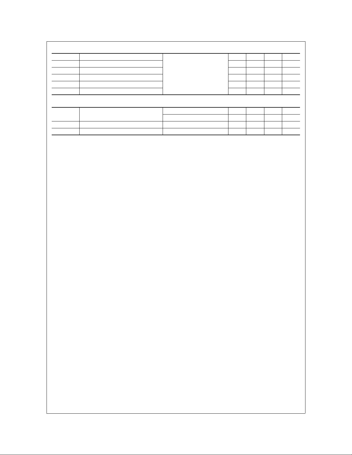
Turn-On Delay Time - 20.3 - ns
Rise Time - 22.0 - ns
Turn-Off Delay Time - 27.1 - ns
Fall Time - 12.1 - ns
Turn-Off Time - - 59.0 ns
GS
= 5V)
Drain-Source Diode Characteristics
V
SD
t
rr
Q
RR
Notes:
1: Starting TJ = 25°C, L = 1mH, IAS = 36A, VDD = 54V, VGS = 10V.
2: Pulse width = 100s.
Source to Drain Diode Voltage
Reverse Recovery Time ISD = 60A, dISD/dt = 100A/µs - - 44 ns
Reverse Recovered Charge ISD = 60A, dISD/dt = 100A/µs - - 57 nC
- - 62.1 ns
VDD = 30V, ID = 80A
VGS = 5V, RGS = 2Ω
I
= 80A - - 1.25 V
SD
ISD = 40A - - 1.0 V
FDB5800 N-Channel Logic Level PowerTrench
This product has been designed to meet the extreme test conditions and environment demanded by the automotive industry. For
All Fairchild Semiconductor products are manufactured, assembled and tested under ISO9000 and QS9000 quality systems
a copy of the requirements, see AEC Q101 at: http://www.aecouncil.com/
certification.
®
MOSFET
FDB5800 Rev. A
www.fairchildsemi.com3
 Loading...