

Fairchild FDB3860 service manual
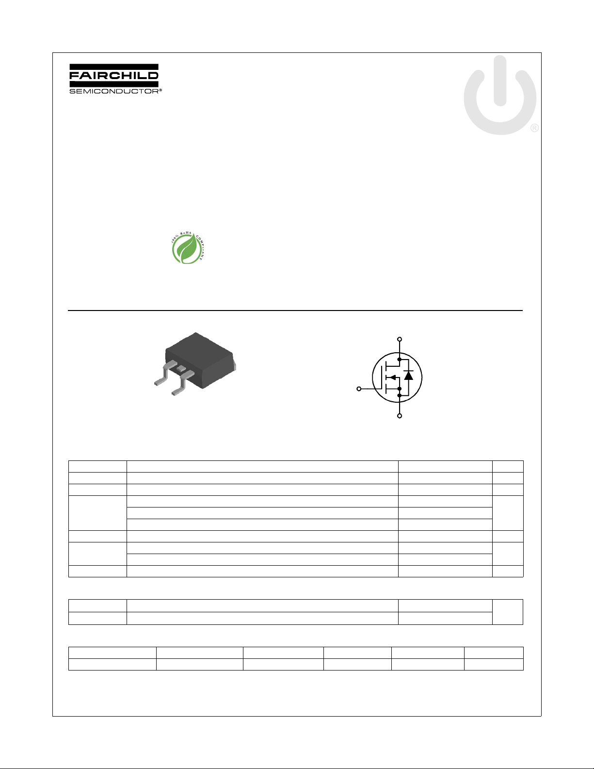
FDB3860
N-Channel PowerTrench® MOSFET
100 V, 30 A, 37 mΩ
Features
Max r
High performance trench technology for extremely low r
100% UIL tested
RoHS Compliant
= 37 mΩ at VGS = 10 V, ID = 5.9 A
DS(on)
DS(on)
General Description
This N-Channel MOSFET is rugged gate version of Fairchild
Semiconductor‘s advanced Power Trench® process. This part is
tailored for low r
ruggedness for a wide range of switching applications
Applications
DC-AC Conversion
Synchronous Rectifier
March 2009
and low Qg figure of merit, with avalanche
DS(on)
FDB3860 N-Channel PowerTrench
.
®
MOSFET
D
G
S
MOSFET Maximum Ratings T
Symbol Parameter Ratings Units
V
DS
V
GS
I
D
E
AS
P
D
, T
T
J
STG
Drain to Source Voltage 100 V
Gate to Source Voltage ±20 V
Drain Current -Continuous (Silicon limited) TC = 25 °C 30
-Pulsed 60
Single Pulse Avalanche Energy (Note 3) 96 mJ
Power Dissipation TC = 25 °C 71
Power Dissipation T
Operating and Storage Junction Temperature Range -55 to +150 °C
TO-263AB
FDB Series
= 25 °C unless otherwise noted
C
= 25 °C (Note 1a) 6.4
A
= 25 °C (Note 1a) 3.1
A
G
D
S
Thermal Characteristics
R
θJC
R
θJA
Thermal Resistance, Junction to Case 1.75
Thermal Resistance, Junction to Ambient (Note 1a) 40
Package Marking and Ordering Information
A -Continuous T
W
°C/W
Device Marking Device Package Reel Size Tape Width Quantity
FDB3860 FDB3860 TO-263AB 330 mm 24 mm 800 units
©2009 Fairchild Semiconductor Corporation
FDB3860 Rev.C
1
www.fairchildsemi.com
FDB3860 N-Channel PowerTrench
Electrical Characteristics T
= 25 °C unless otherwise noted
J
Symbol Parameter Test Conditions Min Typ Max Units
Off Characteristics
BV
∆BV
∆T
I
DSS
I
GSS
DSS
DSS
J
Drain to Source Breakdown Voltage ID = 250 µA, VGS = 0 V 100 V
Breakdown Voltage Temperature
Coefficient
Zero Gate Voltage Drain Current VDS = 80 V, V
Gate to Source Leakage Current VGS = ±20 V, V
I
= 250 µA, referenced to 25 °C 104 mV/°C
D
= 0 V 1 µA
GS
= 0 V ±100 nA
DS
On Characteristics
V
GS(th)
∆V
∆T
r
DS(on)
g
FS
GS(th)
J
Gate to Source Threshold Voltage VGS = VDS, ID = 250 µA 2.5 3.8 4.5 V
Gate to Source Threshold Voltage
Temperature Coefficient
Static Drain to Source On Resistance
I
= 250 µA, referenced to 25 °C -11 mV/°C
D
V
= 10 V, ID = 5.9 A 31 37
GS
= 10 V, ID = 5.9 A, TJ = 125 °C 56 67
V
GS
Forward Transconductance VDS = 10 V, ID = 5.9 A 18 S
Dynamic Characteristics
C
iss
C
oss
C
rss
R
g
Input Capacitance
Output Capacitance 100 130 pF
Reverse Transfer Capacitance 40 65 pF
Gate Resistance 1.7 Ω
Switching Characteristics
t
d(on)
t
r
t
d(off)
t
f
Q
Q
Q
g
gs
gd
Turn-On Delay Time
Rise Time 612ns
Turn-Off Delay Time 17 31 ns
Fall Time 310ns
Total Gate Charge at 10 V
Gate to Source Charge 6.9 nC
Gate to Drain “Miller” Charge 5.4 nC
= 50 V, VGS = 0 V,
V
DS
f = 1 MHz
= 50 V, ID = 5.9 A,
V
DD
V
= 10 V, R
GS
= 50 V, ID = 5.9 A
V
DD
GEN
= 6 Ω
1310 1740 pF
12 22 ns
21 30 nC
mΩ
®
MOSFET
Drain-Source Diode Characteristics
V
SD
t
rr
Q
rr
Notes:
1: R
θJA
R
θJC
a. 40 °C/W when mounted on a 1 in
b. 62.5 °C/W when mounted on a minimum pad.
2: Pulse Test: Pulse Width < 300 µs, Duty cycle < 2.0%.
3: Starting T
©2009 Fairchild Semiconductor Corporation
FDB3860 Rev.C
Source to Drain Diode Forward Voltage
Reverse Recovery Time
Reverse Recovery Charge 37 60 nC
is the sum of the juncti on-t o- cas e a nd cas e-t o -am bi en t th e rma l res ist an ce whe re the ca s e th er ma l ref ere nc e i s de f ine d as the s older mounting surface of the drain pins.
is guaranteed by design while R
= 25 °C, L = 3 mH, IAS = 8 A, VDD = 100 V, VGS = 10 V.
J
is determined by the user’s board design.
θJA
2
pad of 2 oz copper
V
= 0 V, IS = 2.0 A (Note 2) 0.7 1.2
GS
= 0 V, IS = 5.9 A (Note 2) 0.8 1.3
V
GS
= 5.9 A, di/dt = 100 A/µs
I
F
2
35 56 ns
V
www.fairchildsemi.com
 Loading...