

tm
FDB2710
250V N-Channel PowerTrench MOSFET
FDB2710 250V N-Channel PowerTrench MOSFET
November 2006
General Description
This N-Channel MOSFET is produced using Fairchild Semiconductor’s advanced PowerTrench process that has been especially tailored to minimize the on-state resistance and yet
maintain superior switching performance.
Description
• 50A, 250V, R
• Fast switching speed
• Low gate charge
• High performance trench technology for extremely low R
• High power and current handling capability
= 36.3mΩ @VGS = 10 V
DS(on)
Application
• PDP application
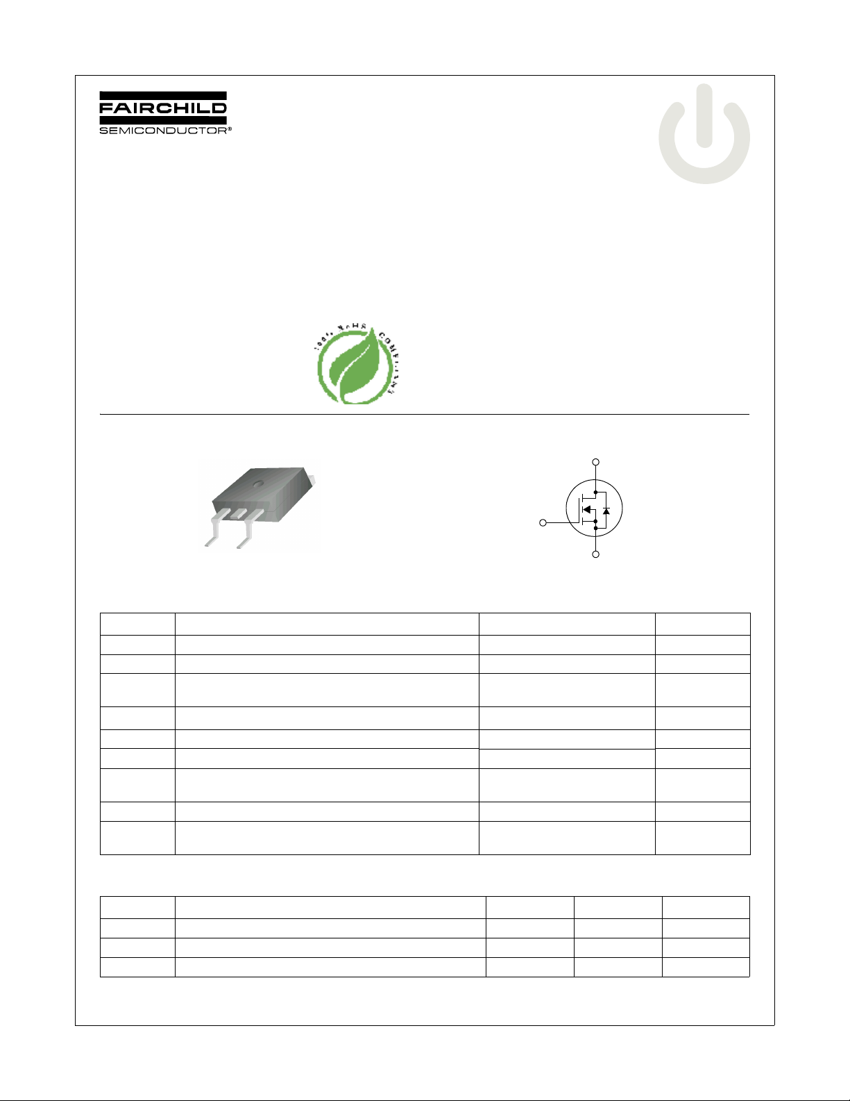
D
G
G
S
D
S
Absolute Maximum Ratings
Symbol Parameter Ratings Unit
V
DS
V
GS
I
D
I
DM
E
AS
dv/dt Peak Diode Recovery dv/dt (Note 3) 4.5 V/ns
P
D
T
J, TSTG
T
L
Drain-Source Voltage 250 V
Gate-Source voltage ± 30 V
Drain Current - Continuous (TC = 25°C)
- Continuous (TC = 100°C)
Drain Current - Pulsed
Single Pulsed Avalanche Energy
Power Dissipation (TC = 25°C)
- Derate above 25°C
Operating and Storage Temperature Range -55 to +150 °C
Maximum Lead Temperature for Soldering Purpose,
1/8” from Case for 5 Seconds
(Note 1)
(Note 2)
50
31.3
See Figure 9
145 mJ
260
2.1
300 °C
W/°C
DS(on)
A
A
A
W
Thermal Characteristics
Symbol Parameter Min Max Unit
R
θJC
R
* Thermal Resistance, Junction-to-Ambient* -- 40 °C/W
θJA
R
θJA
*When mounted on the minimum pad size recommended (PCB Mount)
©2006 Fairchild Semiconductor Corporation 1 www.fairchildsemi.com
FDB2710 Rev. A
Thermal Resistance, Junction-to-Case -- 0.48 °C/W
Thermal Resistance, Junction-to-Ambient -- 62.5 °C/W
Package Marking and Ordering Information
Device Marking Device Package Reel Size Tape Widt h Quantity
FDB2710 FDB2710 D2-Pak 330mm 24mm 800
FDB2710 250V N-Channel PowerTrench MOSFET
Electrical Characteristics T
= 25°C unless otherwise noted
C
Symbol Parameter Conditions Min Typ Max Units
Off Characteristics
BV
DSS
∆BV
/ ∆T
I
DSS
I
GSSF
I
GSSR
On Characteristics
V
GS(th)
R
DS(on)
g
FS
Dynamic Characteristics
C
iss
C
oss
C
rss
Switching Characteristics
t
d(on)
t
r
t
d(off)
t
f
Q
g
Q
gs
Q
gd
Drain-Source Diode Characteristics and Maximum Ratings
I
S
I
SM
V
SD
t
rr
Q
rr
Drain-Source Breakdown Voltage VGS = 0V, ID = 250µA, TJ = 25°C 250 -- -- V
Breakdown Voltage Temperature
DSS
Coefficient
J
Zero Gate Voltage Drain Current VDS = 250V, VGS = 0V
ID = 250µA, Referenced to 25°C -- 0.25 -- V/°C
VDS = 250V, VGS = 0V,TC = 125°C
--
--
--
--
Gate-Body Leakage Current, Forward VGS = 30V, VDS = 0V -- -- 100 nA
Gate-Body Leakage Current, Reverse VGS = -30V, VDS = 0V -- -- -100 nA
Gate Threshold Voltage VDS = VGS, ID = 250µA 3.0 4.0 5.0 V
Static Drain-Source On-Resistance VGS = 10V, ID = 25A -- 36.3 42.5 mΩ
Forward Transconductance VDS = 10V, ID = 25A
Input Capacitance
Output Capacitance -- 426 570 pF
VDS = 25V, VGS = 0V,
f = 1.0MHz
(Note 4)
-- 63 -- S
-- 5470 7280 pF
Reverse Transfer Capacitance -- 97 146 pF
Turn-O n Delay Time VDD = 125V, ID = 50A
Turn-O n Ris e Ti me -- 252 515 ns
VGS = 10V, R
GEN
= 25Ω
-- 80 170 ns
Turn-O ff Delay Time -- 112 235 ns
Turn-O ff Fall Time -- 154 320 ns
Total Gate Charge VDS = 125V, ID = 50A
Gate-Source Charge -- 34 -- nC
VGS = 10V
Gate-Drain Charge -- 18 -- nC
(Note 4, 5)
-- 78 101 nC
(Note 4, 5)
Maximum Continuous Drain-Source Diode Forward Current -- -- 50 A
Maximum Pulsed Drain-Source Diode Forward Current -- -- 150 A
Drain-Source Diode Forward Voltage VGS = 0V, IS = 50A -- -- 1.2 V
Reverse Recovery Time VGS = 0V, IS = 50A
Reverse Recovery Charge -- 1.3 -- µC
dIF/dt =100A/µs (Note 4)
-- 163 -- ns
1
500µAµA
Notes:
1. Repetitive Rating: Pulse width limited by maximum junction temperature
2. L = 1mH, IAS = 17A, VDD = 50V, RG = 25Ω, Starting TJ = 25°C
3. ISD ≤ 50A, di/dt ≤ 100A/µs, VDD ≤ BV
4. Pulse Test: Pulse width ≤ 300µs, Duty Cycle ≤ 2%
5. Essentially Independent of Operating Temperature Typical Characteristics
, Starting TJ = 25°C
DSS
FDB2710 Rev. A
2 www.fairchildsemi.com
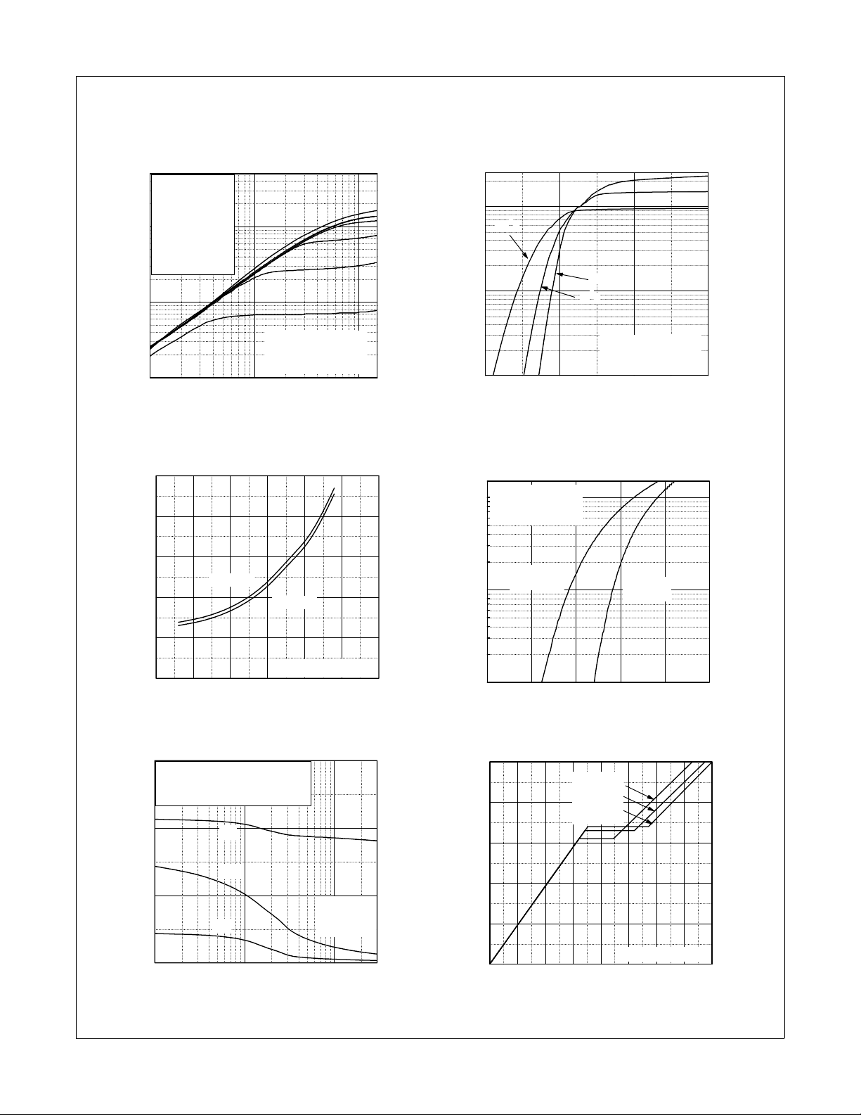
Typical Performance Characteristics
Figure 1. On-Region Characteristics Figure 2. Transfer Characteristics
500
100
V
Top : 15.0 V
10.0 V
8.0 V
7.0 V
6.5 V
6.0 V
Bottom : 5.5 V
GS
10
,Drain Current[A]
D
I
* Notes :
µs Pulse Test
1. 250
= 25oC
2. T
1
0.1 1 10
VDS,Drain-Source Voltage[V]
C
Figure 3. On-Resistance Variation vs. Figure 4. Body Diode Forward Voltage
Drain Current and Gate Voltage Variation vs. Source Current
and Temperatue
0.07
0.06
250
100
150oC
10
,Drain Current[A]
D
I
1
46810
25oC
-55oC
* Notes :
1. V
DS
2. 250
= 20V
µs Pulse Test
VGS,Gate-Source Voltage[V]
150
* Notes :
100
1. V
2. 250
=0V
GS
µs Pulse Test
FDB2710 250V N-Channel PowerTrench MOSFET
0.05
[Ω],
0.04
DS(ON)
R
VGS = 10V
VGS = 20V
0.03
Drain-Source On-Resistance
0.02
0 25 50 75 100 125 150
* Note : TJ = 25oC
ID, Drain Current [A]
10
, Reverse Drain Current [A]
S
I
TA = 150oC
1
0.2 0.4 0.6 0.8 1.0 1.2
TA = 25oC
VSD, Body Diode Forward Voltage [V]
Figure 5. Capacitance Characteristics Figure 6. Gate Charge Characteristics
Capacitances [pF]
9000
6000
3000
C
= Cgs + Cgd (Cds = shorted)
iss
C
= Cds + C
oss
C
= C
rss
gd
0
-1
10
VDS, Drain-Source Voltage [V]
gd
C
iss
C
oss
* Note:
1. V
= 0V
C
rss
0
10
GS
2. f = 1MHz
1
10
30
10
VDS = 50V
V
= 125V
8
V
DS
DS
= 200V
6
4
, Gate-Source Voltage [V]
GS
V
2
0
0 1020304050607080
* Note : ID = 50A
Qg, Total Gate Charge [nC]
FDB2710 Rev. A
3 www.fairchildsemi.com

Typical Performance Characteristics (Continued)
Figure 7. Breakdown Voltage Variation Figure 8. On-Resistance Variation
vs. Temperature vs. Temperature
1.2
2.5
FDB2710 250V N-Channel PowerTrench MOSFET
1.1
2
1.0
, [Normalized]
DSS
BV
0.9
* Notes :
Drain-Source Breakdown Voltage
1. V
2. I
0.8
-100 -50 0 50 100 150 200
TJ, Junction Temperature [oC]
= 0V
GS
= 250µA
D
, [Normalized]
1
DS(on)
r
Drain-Source On-Resistance
0
-100 -50 0 50 100 150 200
* Notes :
1. V
2. I
TJ, Junction Temperature [oC]
Figure 9. Maximum Safe Operating Area Figure 10. Maximum Drain Current
vs. Case Temperature
500
100
10
[A]
D
1
Operation in This Area
is Limited by R
Drain Current, I
0.1
0.01
110100
Drain-Source Voltage, VDS [V]
DS(on)
* Notes :
= 25oC
1. T
C
2. T
= 150oC
J
3. Single Pulse
100µs
1ms
10 ms
DC
400
60
50
40
30
20
, Drain Current [A]
D
I
10
0
25 50 75 100 125 150
TC, Case Temperature [oC]
GS
= 25A
D
= 10V
Figure 11. Transient Thermal Response Curve
P
DM
t
1
* Notes :
(t) = 0.48oC/W Max.
1. Z
θJC
2. Duty Factor, D=t
3. TJM - TC = PDM * Z
-2
10
-1
10
4 www.fairchildsemi.com
FDB2710 Rev. A
0
10
]
0.5
θJC
-1
10
0.2
0.1
0.05
0.02
-2
10
0.01
Thermal Response [Z
Single pulse
-3
10
-5
10
-4
10
-3
10
Rectangular Pulse Duration [sec]
t
2
1/t2
(t)
θJC
0
10
1
10

Gate Charge Test Circuit & Waveform
Resistive Switching Test Circuit & Waveforms
FDB2710 250V N-Channel PowerTrench MOSFET
FDB2710 Rev. A
Unclamped Inductive Switching Test Circuit & Waveforms
5 www.fairchildsemi.com

Peak Diode Recovery dv/dt Test Circuit & Waveforms
FDB2710 250V N-Channel PowerTrench MOSFET
FDB2710 Rev. A
6 www.fairchildsemi.com
FDB2710 250V N-Channel PowerTrench MOSFET
FDB2710 Rev. A
7 www.fairchildsemi.com

TRADEMARKS
The following are registered and unregistered trademarks Fairchild Semiconductor owns or is authorized to use and is not intended to be
an exhaustive list of all such trademarks.
ACEx™
ActiveArray™
Bottomless™
Build it Now™
CoolFET™
CROSSVOLT™
DOME™
EcoSPARK™
2
E
CMOS™
EnSigna™
FACT™
®
FAST
FASTr™
FPS™
FRFET™
FACT Quiet Series™
GlobalOptoisolator™
GTO™
HiSeC™
2
I
C™
i-Lo™
ImpliedDisconnect™
IntelliMAX™
ISOPLANAR™
LittleFET™
MICROCOUPLER™
MicroFET™
MicroPak™
MICROWIRE™
MSX™
MSXPro™
Across the board. Around the world.™
The Power Franchise
®
OCX™
OCXPro™
OPTOLOGIC
®
OPTOPLANAR™
PACMAN™
POP™
Power247™
PowerEdge™
PowerSaver™
PowerTrench
QFET
®
®
QS™
QT Optoelectronics™
Quiet Series™
RapidConfigure™
RapidConnect™
µSerDes™
ScalarPump™
SILENT SWITCHER
SMART START™
SPM™
Stealth™
SuperFET™
SuperSOT™-3
SuperSOT™-6
SuperSOT™-8
SyncFET™
TCM™
TinyBoost™
TinyBuck™
TinyPWM™
TinyPower™
TinyLogic
®
TINYOPTO™
TruTranslation™
UHC™
Programmable Active Droop™
DISCLAIMER
FAIRCHILD SEMICONDUCTOR RESERVES THE RIGHT TO MAKE CHANGES WITHOUT FURTHER NOTICE TO ANY PRODUCTS HEREIN TO
IMPROVE RELIABILITY, FUNCTION OR DESIGN. FAIRCHILD DOES NOT ASSUME ANY LIABILITY ARISING OUT OF THE APPLICATION OR USE OF
ANY PRODUCT OR CIRCUIT DESCRIBED HEREIN; NEITHER DOES IT CONVEY ANY LICENSE UNDER ITS PATENT RIGHTS, NOR THE RIGHTS OF
OTHERS. THESE SPECIFICATIONS DO NOT EXPAND THE TERMS OF FAIRCHILD’S WORLDWIDE TERMS AND CONDITIONS, SPECIFICALLY THE
WARRANTY THEREIN, WHICH COVERS THESE PRODUCTS.
®
UniFET™
UltraFET
VCX™
Wire™
®
FDB2710 250V N-Channel PowerTrench MOSFET
LIFE SUPPORT POLICY
FAIRCHILD’S PRODUCTS ARE NOT AUTHORIZED FOR USE AS CRITICAL COMPONENTS IN LIFE SUPPORT DEVICES OR SYSTEMS WITHOUT
THE EXPRESS WRITTEN APPROVAL OF FAIRCHILD SEMICONDUCTOR CORPORATION.
As used herein:
1. Life support devices or systems are devices or systems which,
(a) are intended for surgical implant into the body, or (b) support
or sustain life, or (c) whose failure to perform when properly used
in accordance with instructions for use provided in the labeling,
2. A critical component is any component of a life support device
or system whose failure to perform can be reasonably expected to
cause the failure of the life support device or system, or to affect
its safety or effectiveness.
can be reasonably expected to result in significant injury to the
user.
PRODUCT STATUS DEFINITIONS
Definition of Terms
Datasheet Identification Product Status Definition
Advance Information Formative or In
Design
This datasheet contains the design specifications for
product development. Specifications may change in
any manner without notice.
Preliminary First Production This datasheet contains preliminary data, and
supplementary data will be published at a later date.
Fairchild Semiconductor reserves the right to make
changes at any time without notice in order to improve
design.
No Identification Needed Full Production This datasheet contains final specifications. Fairchild
Semiconductor reserves the right to make changes at
any time without notice in order to improve design.
Obsolete Not In Production This datasheet contains specifications on a product
that has been discontinued by Fairchild semiconductor.
The datasheet is printed for reference information only.
FDB2710 Rev. A
8 www.fairchildsemi.com
Rev. I20
 Loading...