

tm
FDA20N50F
D
G
S
TO-3PN
GSD
N-Channel MOSFET
500V, 22A, 0.26Ω
FDA20N50F N-Channel MOSFET
January 2012
TM
UniFET
Features
•R
• Low gate charge ( Typ. 50nC )
• Low C
• Fast switching
• 100% avalanche tested
• Improved dv/dt capability
• RoHS compliant
MOSFET Maximum Ratings T
V
DSS
V
GSS
I
D
I
DM
E
AS
I
AR
E
AR
dv/dt Peak Diode Recovery dv/dt (Note 3) 20 V/ns
P
D
, T
T
J
T
L
= 0.22Ω ( Typ.) @ VGS = 10V, ID = 11A
DS(on)
( Typ. 27pF )
rss
= 25oC unless otherwise noted*
C
Symbol Parameter Ratings Units
Drain to Source Voltage 500 V
Gate to Source Voltage ±30 V
-Continuous (T
-Continuous (T
(T
= 25oC) 388 W
C
- Derate above 25
STG
D r a i n C u r r e n t
D r a i n C u r r e n t - P u l s e d (Note 1) 88 A
Single Pulsed Avalanche Energy (Note 2) 1110 mJ
Avalanche Current (Note 1) 22 A
Repetitive Avalanche Energy (Note 1) 39 mJ
Power Dissipation
Operating and Storage Temperature Range -55 to +150
Maximum Lead Temperature for Soldering Purpose,
1/8” from Case for 5 Seconds
Description
These N-Channel enhancement mode power field effect
transistors are produced using Fairchild’s proprietary, planar
stripe, DMOS technology.
This advance technology has been especially tailored to
minimize on-state resistance, provide superior switching
performance, and withstand high energy pulse in the avalanche
and commutation mode. These device are well suited for high
efficient switched mode power supplies and active power factor
correction.
= 25oC) 22
C
= 100oC) 13
C
o
C3.1W/
300
o
o
A
o
C
C
C
Thermal Characteristics
Symbol Parameter Min. Max. Units
R
θJC
θCS
R
θJA
©2012 Fairchild Semiconductor Corporation
FDA20N50F Rev.C0
Thermal Resistance, Junction to Case - 0.44
Thermal Resistance, Case to Sink 0.24 -
Thermal Resistance, Junction to Ambient - 40
o
C/WR
www.fairchildsemi.com1
Package Marking and Ordering Information
Device Marking Device Package Reel Size Tape Width Quantity
FDA20N50F FDA20N50F TO-3PN - - 30
FDA20N50F N-Channel MOSFET
Electrical Characteristics T
= 25oC unless otherwise noted
C
Symbol Parameter Test Conditions Min. Typ. Max. Units
Off Characteristics
BV
DSS
ΔBV
/ ΔT
I
DSS
I
GSS
DSS
J
Drain to Source Breakdown Voltage ID = 250μA, VGS = 0V, TJ = 25oC500 - - V
Breakdown Voltage Temperature
Coefficient
Zero Gate Voltage Drain Current
Gate to Body Leakage Current VGS = ±30V, V
I
= 250μA, Referenced to 25oC-0.6-V/
D
V
= 500V, V
DS
= 400V, TC = 125oC - - 100
V
DS
= 0V - - 10
GS
= 0V - - ±100 nA
DS
On Characteristics
V
R
g
GS(th)
FS
DS(on)
Gate Threshold Voltage VGS = VDS, ID = 250μA 3.0 - 5.0 V
Static Drain to Source On Resistance VGS = 10V, ID = 11A - 0.22 0.26 Ω
Forward Transconductance VDS = 40V, ID = 11A (Note 4) -24-S
Dynamic Characteristics
C
C
C
Q
Q
Q
iss
oss
rss
g(tot)
gs
gd
Input Capacitance
Output Capacitance - 350 465 pF
Reverse Transfer Capacitance - 27 40 pF
Total Gate Charge at 10V
Gate to Source Gate Charge - 14 - nC
Gate to Drain “Miller” Charge - 20 - nC
Switching Characteristics
t
d(on)
t
r
t
d(off)
t
f
Turn-On Delay Time
Turn-On Rise Time - 120 250 ns
Turn-Off Delay Time - 100 210 ns
Turn-Off Fall Time - 60 130 ns
= 25V, VGS = 0V
V
DS
f = 1MHz
V
= 400V, ID = 20A
DS
V
= 10V
GS
(N ote 4, 5)
= 250V, ID = 20A
V
DD
R
= 25Ω
G
(N ote 4 , 5)
- 2550 3390 pF
-5065nC
- 45 100 ns
μA
o
C
Drain-Source Diode Characteristics
I
S
I
SM
V
SD
t
rr
Q
rr
Notes:
1: Repetitive Rating: Pulse width limited by maximum junction temperature
2: L = 5mH, IAS = 20A, VDD = 50V, RG = 25Ω, Starting TJ = 25°C
3: ISD ≤ 22A, di/dt ≤ 200A/μs, VDD ≤ BV
4: Pulse Test: Pulse width ≤ 300μs, Duty Cycle ≤ 2%
5: Essentially Independent of Operating Temperature Typical Characteristics
FDA20N50F Rev.C0
Maximum Continuous Drain to Source Diode Forward Current - - 22 A
Maximum Pulsed Drain to Source Diode Forward Current - - 88 A
Drain to Source Diode Forward Voltage V
Reverse Recovery Time
Reverse Recovery Charge - 0.5 - μC
, Starting TJ = 25°C
DSS
= 0V, I
GS
V
= 0V, I
GS
dI
/dt = 100A/μs (Note 4)
F
= 22A - - 1.5 V
SD
= 20A
SD
2
- 154 - ns
www.fairchildsemi.com
Typical Performance Characteristics
0.1 1 10
1
10
0.5
*Notes:
1. 250
μs Pulse Test
2. T
C
= 25oC
V
GS
= 15.0 V
10.0 V
8.0 V
7.0 V
6.5 V
6.0 V
5.5 V
I
D
,Drain Current[A]
VDS,Drain-Source Voltage[V]
80
468
1
10
100
150oC
*Notes:
1. V
DS
= 20V
2. 250
μs Pulse Test
25oC
I
D
,Drain Current[A]
VGS,Gate-Source Voltage[V]
0.0 0.5 1.0 1.5
1
10
100
*Notes:
1. VGS = 0V
2. 250
μs Pulse Test
150oC
I
S
, Reverse Drain Current [A]
VSD, Body Diode Forward Voltage [V]
25oC
0.2
0 255075
0.1
0.2
0.3
0.4
0.5
0.6
0.7
0.8
*Note: TJ = 25oC
VGS = 20V
VGS = 10V
R
DS(ON)
[Ω],
Drain-Source On-Resistance
ID, Drain Current [A]
0.1 1 10
0
1500
3000
4500
6000
C
oss
C
iss
C
iss
= Cgs + Cgd (Cds = shorted)
C
oss
= Cds + C
gd
C
rss
= C
gd
*Note:
1. V
GS
= 0V
2. f = 1MHz
C
rss
Capacitances [pF]
VDS, Drain-Source Voltage [V]
50
0 102030405060
0
2
4
6
8
10
*Note: ID = 20A
VDS = 100V
V
DS
= 250V
V
DS
= 400V
V
GS
, Gate-Source Voltage [V]
Qg, Total Gate Charge [nC]
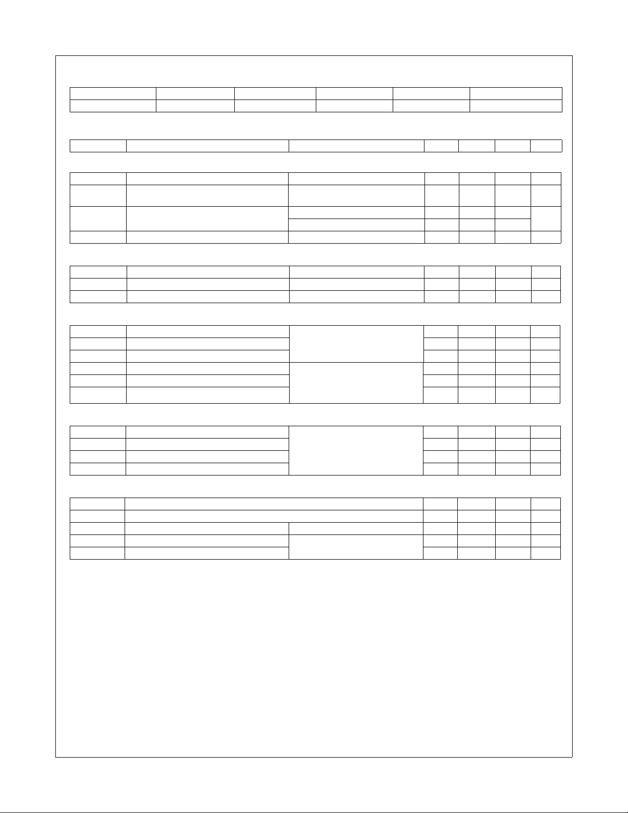
Figure 1. On-Region Characteristics Figure 2. Transfer Characteristics
Figure 3. On-Resistance Variation vs. Figure 4. Body Diode Forward Voltage
Drain Current and Gate Voltage Variation vs. Source Current
and Temperature
FDA20N50F N-Channel MOSFET
Figure 5. Capacitance Characteristics Figure 6. Gate Charge Characteristics
FDA20N50F Rev.C0
3
www.fairchildsemi.com
Typical Performance Characteristics (Continued)
-100 -50 0 50 100 150 200
0.8
0.9
1.0
1.1
1.2
*Notes:
1. V
GS
= 0V
2. I
D
= 250μA
BV
DSS
, [Normalized]
Drain-Source Breakdown Voltage
TJ, Junction Temperature [oC]
1 10 100 1000
0.1
1
10
100
30μs
100μs
1ms
10ms
I
D
, Drain Current [A]
VDS, Drain-Source Voltage [V]
Operation in This Area
is Limited by R
DS(on)
*Notes:
1. T
C
= 25oC
2. T
J
= 150oC
3. Single Pulse
DC
200
25 50 75 100 125 150
0
5
10
15
20
25
I
D
, Drain Current [A]
TC, Case Temperature [oC]
10
-5
10
-4
10
-3
10
-2
10
-1
10
0
1E-3
0.01
0.1
1
0.01
0.1
0.2
0.05
0.02
*Notes:
1. Z
θJC
(t) = 0.44oC/W Max.
2. Duty Factor, D=t
1/t2
3. TJM - TC = PDM * Z
θJC
(t)
0.5
Single pulse
Thermal Response [Z
θJC
]
Rectangular Pulse Duration [sec]
t
1
P
DM
t
2
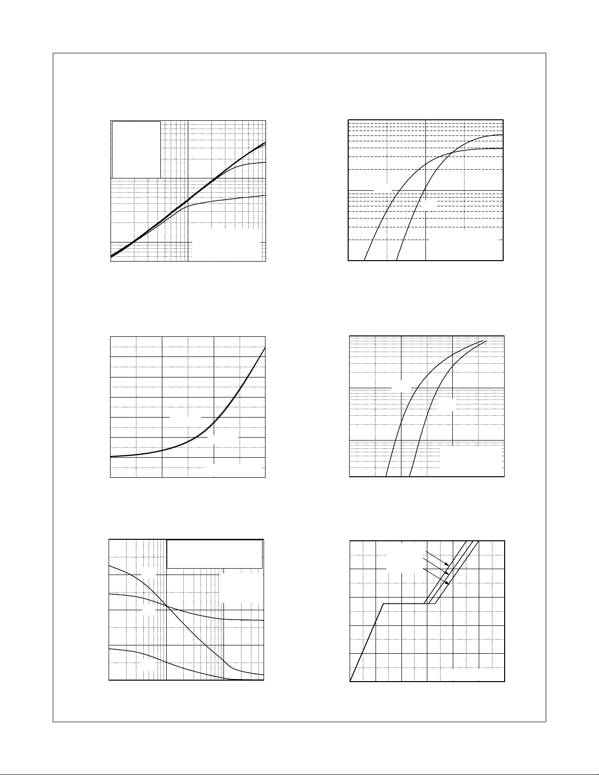
Figure 7. Breakdown Voltage Variation Figure 8. Maximum Safe Operating Area
vs. Temperature
Figure 9. Maximum Drain Current
vs. Case Temperature
FDA20N50F N-Channel MOSFET
Figure 10. Transient Thermal Response Curve
FDA20N50F Rev.C0
4
www.fairchildsemi.com

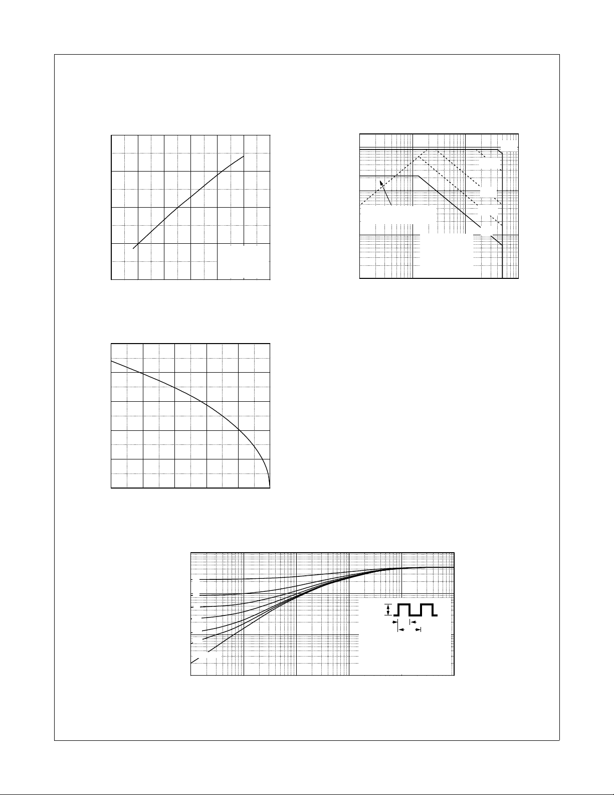
Gate Charge Test Circuit & Waveform
Resistive Switching Test Circuit & Waveforms
Unclamped Inductive Switching Test Circuit & Waveforms
FDA20N50F N-Channel MOSFET
FDA20N50F Rev.C0
5
www.fairchildsemi.com

DUT
V
DS
+
_
Driver
R
G
Same Type
as DUT
V
GS
• dv/dt controlled by R
G
•ISDcontrolled by pulse period
V
DD
L
I
SD
10V
V
GS
( Driver )
I
SD
( DUT )
V
DS
( DUT )
V
DD
Body Diode
Forward Voltage Drop
V
SD
IFM, Body Diode Forward Current
Body Diode Reverse Current
I
RM
Body Diode Recovery dv/dt
di/dt
D =
Gate Pulse Width
Gate Pulse Period
--------------------------
DUT
V
DS
+
_
Driver
R
G
Same Type
as DUT
V
GS
• dv/dt controlled by R
G
•ISDcontrolled by pulse period
V
DD
LL
I
SD
10V
V
GS
( Driver )
I
SD
( DUT )
V
DS
( DUT )
V
DD
Body Diode
Forward Voltage Drop
V
SD
IFM, Body Diode Forward Current
Body Diode Reverse Current
I
RM
Body Diode Recovery dv/dt
di/dt
D =
Gate Pulse Width
Gate Pulse Period
--------------------------
D =
Gate Pulse Width
Gate Pulse Period
--------------------------
FDA20N50F N-Channel MOSFET
Peak Diode Recovery dv/dt Test Circuit & Waveforms
FDA20N50F Rev.C0
6
www.fairchildsemi.com

Mechanical Dimensions
FDA20N50F N-Channel MOSFET
TO-3PN
FDA20N50F Rev.C0
7
www.fairchildsemi.com
TRADEMARKS
®
™
tm
tm
The following includes registered and unregistered trademarks and service marks, owned by Fairchild Semiconductor and/or its global subsidiaries, and is not
intended to be an exhaustive list of all such trademarks.
2Cool™
AccuPower™
AX-CAP™*
®
BitSiC
Build it Now™
CorePLUS™
CorePOWER™
CROSSVOLT™
CTL™
Current Transfer Logic™
DEUXPEED
Dual Cool™
EcoSPARK
EfficentMax™
®
®
ESBC™
®
Fairchild
Fairchild Semiconductor
FACT Quiet Series™
®
FACT
®
FAST
FastvCore™
FETBench™
FlashWriter
®
*
FPS™
®
F-PFS™
®
FRFET
Global Power Resource
Green Bridge™
Green FPS™
Green FPS™ e-Series™
max™
G
GTO™
IntelliMAX™
ISOPLANAR™
Marking Small Speakers Sound Louder
and Better™
MegaBuck™
MICROCOUPLER™
MicroFET™
MicroPak™
MicroPak2™
MillerDrive™
MotionMax™
Motion-SPM™
mWSaver™
OptoHiT™
OPTOLOGIC
OPTOPLANAR
®
®
®
SM
PowerTrench
PowerXS™
Programmable Active Droop™
QFET
QS™
Quiet Series™
RapidConfigure™
Saving our world, 1mW/W/kW at a time™
SignalWise™
SmartMax™
SMART START™
Solutions for Your Success™
SPM
STEALTH™
SuperFET
SuperSOT™-3
SuperSOT™-6
SuperSOT™-8
SupreMOS
SyncFET™
Sync-Lock™
®
®
®
®
®
®*
The Power Franchise
TinyBoost™
TinyBuck™
TinyCalc™
®
TinyLogic
TINYOPTO™
TinyPower™
TinyPWM™
TinyWire™
®
TranSiC
TriFault Detect™
TRUECURRENT
μSerDes™
®
UHC
Ultra FRFET™
UniFET™
VCX™
VisualMax™
VoltagePlus™
XS™
®
®
®
*
*Trademarks of System General Corporation, used under license by Fairchild Semiconductor.
DISCLAIMER
FAIRCHILD SEMICONDUCTOR RESERVES THE RIGHT TO MAKE CHANGES WITHOUT FURTHER NOTICE TO ANY PRODUCTS HEREIN TO IMPROVE
RELIABILITY, FUNCTION, OR DESIGN. FAIRCHILD DOES NOT ASSUME ANY LIABILITY ARISING OUT OF THE APPLICATION OR USE OF ANY PRODUCT
OR CIRCUIT DESCRIBED HEREIN; NEITHER DOES IT CONVEY ANY LICENSE UNDER ITS PATENT RIGHTS, NOR THE RIGHTS OF OTHERS. THESE
SPECIFICATIONS DO NOT EXPAND THE TERMS OF FAIRCHILD’S WORLDWIDE TERMS AND CONDITIONS, SPECIFICALLY THE WARRANTY THEREIN,
WHICH COVERS THESE PRODUCTS.
FDA20N50F N-Channel MOSFET
LIFE SUPPORT POLICY
FAIRCHILD’S PRODUCTS ARE NOT AUTHORIZED FOR USE AS CRITICAL COMPONENTS IN LIFE SUPPORT DEVICES OR SYSTEMS WITHOUT THE
EXPRESS WRITTEN APPROVAL OF FAIRCHILD SEMICONDUCTOR CORPORATION.
As used here in:
1. Life support devices or systems are devices or systems which, (a) are
intended for surgical implant into the body or (b) support or sustain life,
and (c) whose failure to perform when properly used in accordance with
instructions for use provided in the labeling, can be reasonably
expected to result in a significant injury of the user.
ANTI-COUNTERFEITING POLICY
Fairchild Semiconductor Corporation’s Anti-Counterfeiting Policy. Fairchild’s Anti-Counterfeiting Policy is also stated on our external website,
www.Fairchildsemi.com, under Sales Support
Counterfeiting of semiconductor parts is a growing problem in the industry. All manufactures of semiconductor products are experiencing counterfeiting of their
parts. Customers who inadvertently purchase counterfeit parts experience many problems such as loss of brand reputation, substandard performance, failed
application, and increased cost of production and manufacturing delays. Fairchild is taking strong measures to protect ourselves and our customers from the
proliferation of counterfeit parts. Fairchild strongly encourages customers to purchase Fairchild parts either directly from Fairchild or from Authorized Fairchild
Distributors who are listed by country on our web page cited above. Products customers buy either from Fairchild directly or from Authorized Fairchild
Distributors are genuine parts, have full traceability, meet Fairchild’s quality standards for handing and storage and provide access to Fairchild’s full range of
up-to-date technical and product information. Fairchild and our Authorized Distributors will stand behind all warranties and will appropriately address and
warranty issues that may arise. Fairchild will not provide any warranty coverage or other assistance for parts bought from Unauthorized Sources. Fairchild is
.
2. A critical component in any component of a life support, device, or
system whose failure to perform can be reasonably expected to cause
the failure of the life support device or system, or to affect its safety or
effectiveness.
committed to combat this global problem and encourage our customers to do their part in stopping this practice by buying direct or from authorized distributors.
PRODUCT STATUS DEFINITIONS
Definition of Terms
Datasheet Identification Product Status Definition
Advance Information Formative / In Design
Preliminary First Production
No Identification Needed Full Production
Obsolete Not In Production
FDA20N50F Rev.C0
Datasheet contains the design specifications for product development. Specifications
may change in any manner without notice.
Datasheet contains preliminary data; supplementary data will be published at a later
date. Fairchild Semiconductor reserves the right to make changes at any time without
notice to improve design.
Datasheet contains final specifications. Fairchild Semiconductor reserves the right to
make changes at any time without notice to improve the design.
Datasheet contains specifications on a product that is discontinued by Fairchild
Semiconductor. The datasheet is for reference information only.
8
www.fairchildsemi.com
Rev. I61
 Loading...