FAN3278
30V PMOS-NMOS Bridge Driver
FAN3278 — 30V PMOS-NMOS Bridge Driver
July 2012
Features
8V to 27V Optimum Operating Range
Drives High-Side PMOS and Low-Side NMOS in
Motor Control or Buck Step-Down Applications
Output Drive-Voltage Magnitude Limited: < 13V
for V
up to 30V
DD
Biases Each Load Device OFF with a 100kΩ
Resistor when V
Below Operating Level
DD
Low-Voltage TTL Input Thresholds
Peak Gate Drives at 12V: +1.5A Sink, -1.0A Source
Internal Resistors Hold Driver Off When
No Inputs Present
8-Lead SOIC Package
Rated from –40°C to +125°C Ambient
Applications
Motor Control with PMOS / NMOS Half-Bridge
Configuration
Buck Converters with High-Side PMOS Device;
100% Duty Cycle Operation Possible
Logic-Controlled Load Circuits with High-Side
PMOS Switch
Description
The FAN3278 dual 1.5A gate driver is optimized to drive
a high-side P-channel MOSFET and a low-side
N-channel MOSFET in motor control applications
operating from a voltage rail up to 27V. Internal circuitry
limits the voltage applied to the gates of the external
MOSFETs to 13V maximum. The driver has TTL input
thresholds and provides buffer and level translation from
logic inputs. Internal circuitry prevents the output
switching devices from operating if the VDD supply
voltage is below the IC operation level. Internal 100kΩ
resistors bias the non-inverting output LOW and the
inverting output to V
off during startup intervals when logic control signals
may not be present.
The FAN3278 driver incorporates MOSFET devices for
the final output stage, providing high current throughout
the MOSFET turn-on / turn-off transition to minimize
switching loss. The internal gate-drive regulators
provide optimum gate-drive voltage when operating
from a rail of 8V to 27V. The FAN3278 can be driven
from a voltage rail of less than 8V; however, its gate
drive current is reduced.
The FAN3278 has two independent ENABLE pins that
default to ON if not connected. If the ENABLE pin for
non-inverting channel A is pulled LOW, OUTA is forced
LOW. If the ENABLE pin for inverting channel B is
pulled LOW, OUTB is forced HIGH. If an input is left
unconnected, internal resistors bias the inputs such that
the external MOSFETs are OFF.
to keep the external MOSFETs
DD
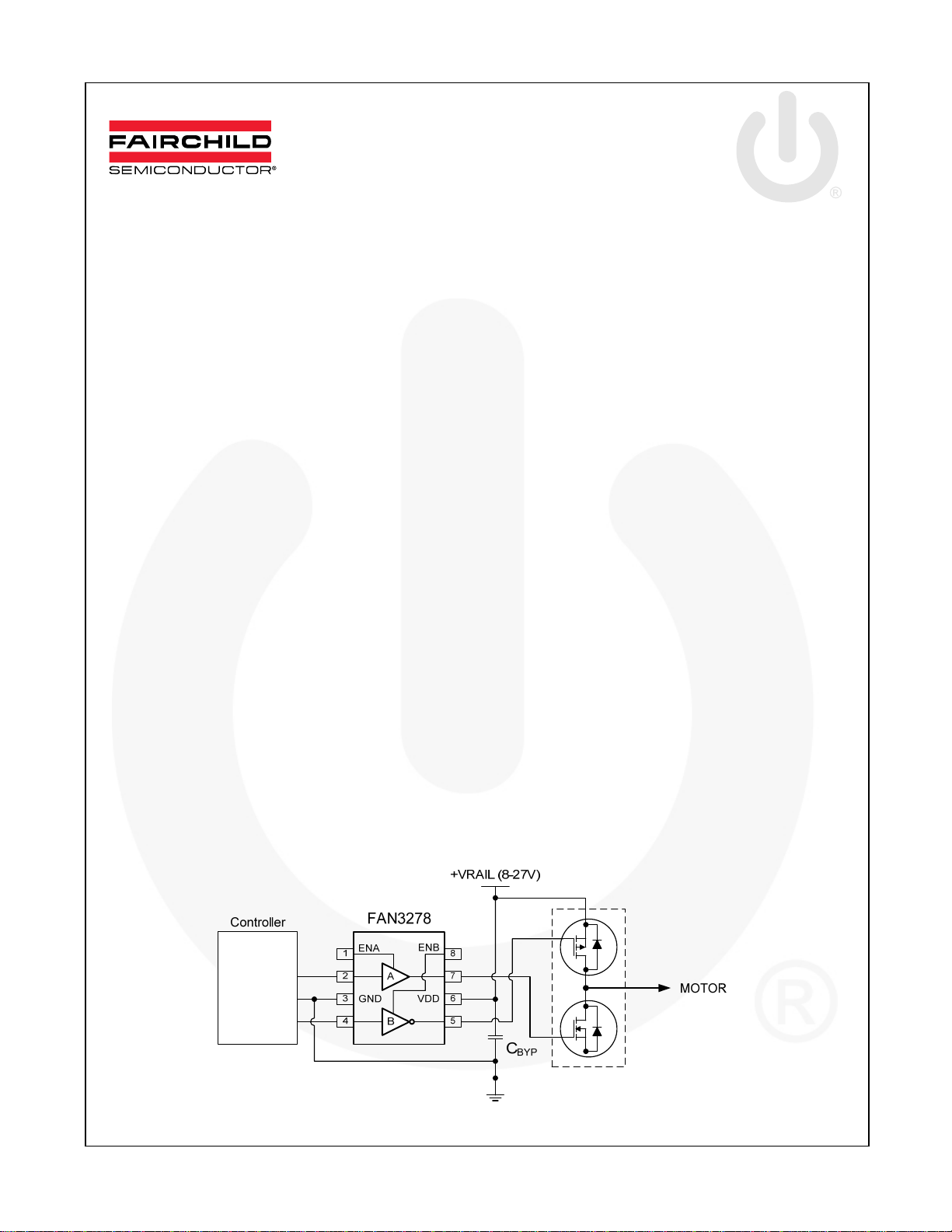
Figure 1. Typical Application
© 2010 Fairchild Semiconductor Corporation www.fairchildsemi.com
FAN3278 • Rev. 1.0.1

Ordering Information
FAN3278 — 30V PMOS-NMOS Bridge Driver
Part Number Logic
FAN3278TMX Non-Inverting Channel and Inverting Channel with Dual Enable TTL
Input
Threshold
Packing
Method
2,500 Units on
Tape & Reel
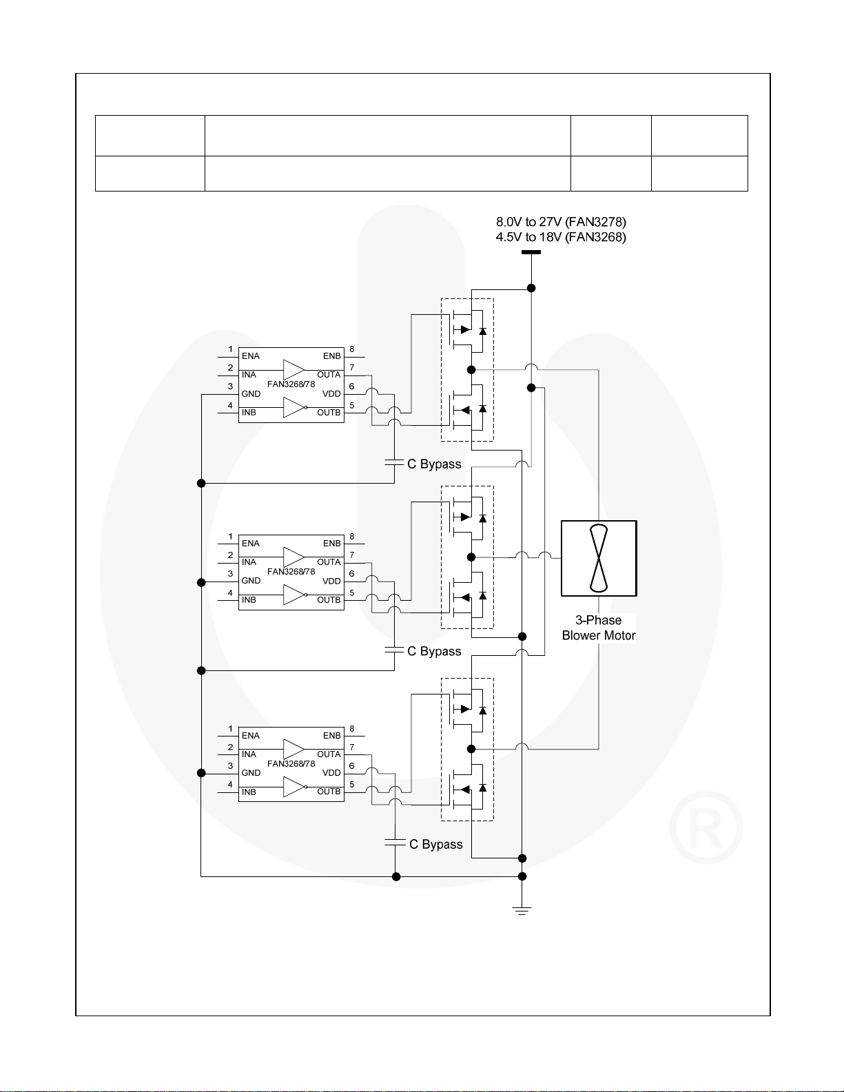
Figure 2. Typical 3-Phase Blower Motor Dri ve Application
© 2010 Fairchild Semiconductor Corporation www.fairchildsemi.com
FAN3278 • Rev. 1.0.1 2

Pin Configuration
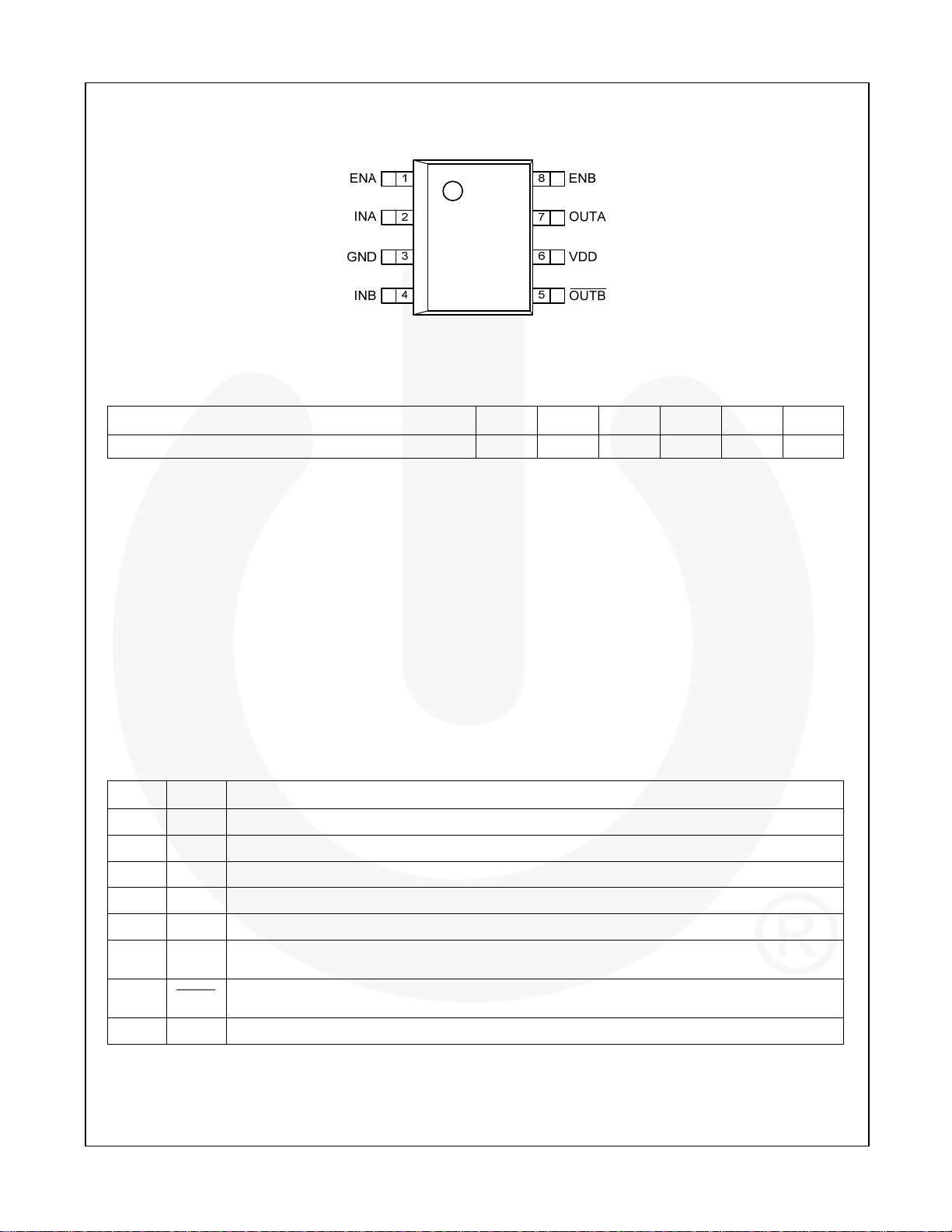
Figure 3. Pin Configuration (Top View)
(1)
Thermal Characteristics
Package
8-Pin Small-Outline Integrated Circuit (SOIC)
Notes:
1. Estimates derived from thermal simulation; actual values depend on the application.
2. Theta_JL (ΘJL): Thermal resistance between the semiconductor junction and the bottom surface of all the leads
(including any thermal pad) that are typically soldered to a PCB.
3. Theta_JT (Θ
assuming it is held at a uniform temperature by a top-side heatsink.
4. Theta_JA (Θ
and airflow. The value given is for natural convection with no heatsink, as specified in JEDEC standards
JESD51-2, JESD51-5, and JESD51-7, as appropriate.
5. Psi_JB (ΨJB): Thermal characterization parameter providing correlation between semiconductor junction
temperature and an application circuit board reference point for the thermal environment defined in Note 4. For
the SOIC-8 package, the board reference is defined as the PCB copper adjacent to pin 6.
6. Psi_JT (Ψ
temperature and the center of the top of the package for the thermal environment defined in Note 4.
): Thermal resistance between the semiconductor junction and the top surface of the package,
JT
): Thermal resistance between junction and ambient, dependent on the PCB design, heat sinking,
JA
): Thermal characterization parameter providing correlation between the semiconductor junction
JT
(2)
Θ
Θ
JL
40 31 89 43 3 °C/W
JT
(3)
Θ
JA
(4)
Ψ
JB
(5)
Ψ
(6)
Unit
JT
FAN3278 — 30V PMOS-NMOS Bridge Driver
Pin Definitions
Pin# Name Description
1 ENA Enable Input for Channel A. Pull pin LOW to inhibit driver A. ENA has TTL thresholds.
8 ENB Enable Input for Channel B. Pull pin LOW to inhibit driver B. ENB has TTL thresholds.
3 GND Ground. Common ground reference for input and output circuits.
2 INA Input to Channel A.
4 INB
7
OUTA
5
OUTB
6 VDD Supply Voltage. Provides power to the IC.
© 2010 Fairchild Semiconductor Corporation www.fairchildsemi.com
FAN3278 • Rev. 1.0.1 3
Input to Channel B.
Gate Drive Output A: Held LOW unless required input is present and V
is above the internal
DD
voltage threshold where the IC is functional.
Gate Drive Output B (inverted from the input). Held HIGH unless the required input is present
and V
is above the internal voltage threshold where the IC is functional.
DD

Output Logic
FAN3278 (Channel A) FAN3278 (Channel B)
FAN3278 — 30V PMOS-NMOS Bridge Driver
ENA INA OUTA ENB INB
0 0
(7)
0 0 0
(7)
1
0 1 0 0 1 1
(7)
1
0
(7)
1
1 1 1
(7)
0 1
(7)
0
(7)
1 0
(7)
1
Note:
7. Default input signal if no external connection is made.
Block Diagram
V
DD
100k
1
ENA
INA
2
13V
LS
Predriver
OUTB
V
DD
100k
8
ENB
OUTA
7
GND
INB
100k
100k
Low-Side
Drive
Regulator
6
3
VDD
High-Side
Drive
Regulator
HS
4
100k
-13V
V
DD
Predriver
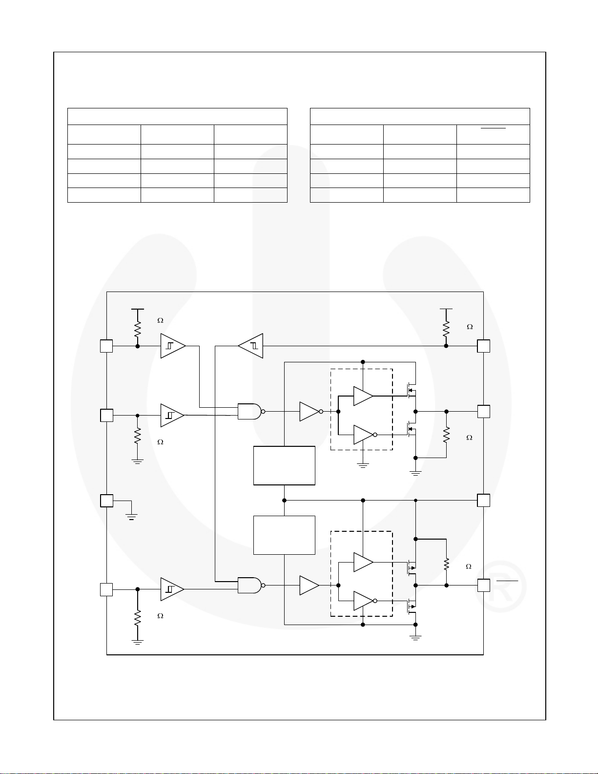
Figure 4. Block Diagram
100k
5
OUTB
© 2010 Fairchild Semiconductor Corporation www.fairchildsemi.com
FAN3278 • Rev. 1.0.1 4

Absolute Maximum Ratings
Stresses exceeding the absolute maximum ratings may damage the device. The device may not function or be
operable above the recommended operating conditions and stressing the parts to these levels is not recommended.
In addition, extended exposure to stresses above the recommended operating conditions may affect device reliability.
The absolute maximum ratings are stress ratings only.
Symbol Parameter Min. Max. Unit
VDD VDD to PGND -0.3 30.0 V
VEN ENA, ENB to GND GND - 0.3 VDD + 0.3 V
VIN INA, INB to GND GND - 0.3 VDD + 0.3 V
V
OUTA, OUTB to GND GND - 0.3 VDD + 0.3 V
OUT
TL Lead Soldering Temperature (10 Seconds) +260 ºC
TJ Junction Temperature -55 +150 ºC
T
Storage Temperature -65 +150 ºC
STG
Recommended Operating Conditions
The Recommended Operating Conditions table defines the conditions for actual device operation. Recommended
operating conditions are specified to ensure optimal performance to the datasheet specifications. Fairchild does not
recommend exceeding them or designing to Absolute Maximum Ratings.
FAN3278 — 30V PMOS-NMOS Bridge Driver
Symbol Parameter Min. Max. Unit
VDD Supply Voltage Range 8 27 V
VEN Enable Voltage (ENA, ENB) 0 VDD V
VIN Input Voltage (INA, INB) 0 VDD V
TA Operating Ambient Temperature -40 +125 °C
© 2010 Fairchild Semiconductor Corporation www.fairchildsemi.com
FAN3278 • Rev. 1.0.1 5
 Loading...