FAN3111 — Single 1A High-Speed, Low-Side
Gate Driver
FAN3111 — Single 1A High-Speed, Low-Side Gate Driver
July 2012
Features
1.4A Peak Sink / Source at VDD = 12V
1.1A Sink / 0.9A Source at V
OUT
= 6V
4.5 to 18V Operating Range
FAN3111C Compatible with FAN3100C Footprint
Two Input Configurations:
Dual CMOS Inputs Allow Configuration as
Non-Inverting or Inverting with Enable Function
Single Non-Inverting, Low-Voltage Input for
Compatibility with Low-Voltage Controllers
Small Footprint Facilitates Distributed Drivers for
Parallel Power Devices
15ns Typical Delay Times
9ns Typical Rise / 8ns Typical Fall times with 470pF
Load
5-Pin SOT23 Package
Rated from –40°C to 125°C Ambient
Applications
Switch-Mode Power Supplies
Synchronous Rectifier Circuits
Pulse Transformer Driver
Logic to Power Buffer
Motor Control
Description
The FAN3111 1A gate driver is designed to drive an Nchannel enhancement-mode MOSFET in low-side
switching applications.
Two input options are offered: FAN3111C has dual
CMOS inputs with thresholds referenced to V
with PWM controllers and other input-signal sources that
operate from the same supply voltage as the driver. For
use with low-voltage controllers and other input-signal
sources that operate from a lower supply voltage than
the driver, that supply voltage may also be used as the
reference for the input thresholds of the FAN3111E.
This driver has a single, non-inverting, low-voltage input
plus a DC input V
in the range 2 to 5V.
The FAN3111 is available in a lead-free finish industrystandard 5-pin SOT23.
for an external reference voltage
XREF
for use
DD
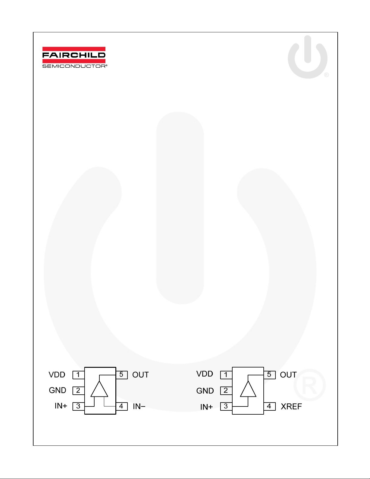
Figure 1. FAN3111C (Top View)
© 2008 Fairchild Semiconductor Corporation www.fairchildsemi.com
FAN3111 • Rev. 1.0.3
Figure 2. FAN3111E (Top View)

Ordering Information
FAN3111 — Single 1A High-Speed, Low-Side Gate Driver
Part Number
Input
Threshold
Package Packing Method
Quantity per
Reel
FAN3111CSX CMOS 5-Pin SOT23 Tape & Reel 3,000
(2)
Θ
Tape & Reel
(3)
Θ
JT
JA
(4)
Ψ
JB
(5)
Ψ
3,000
(6)
JT
Units
FAN3111ESX External 5-Pin SOT23
Thermal Characteristics
(1)
Package
5-Pin SOT23
Θ
JL
58 102 161 53 6 °C/W
Notes:
1. Estimates derived from thermal simulation; actual values depend on the application.
2. Theta_JL (Θ
): Thermal resistance between the semiconductor junction and the bottom surface of all the leads
JL
(including any thermal pad) that are typically soldered to a PCB.
3. Theta_JT (ΘJT): Thermal resistance between the semiconductor junction and the top surface of the package,
assuming it is held at a uniform temperature by a top-side heatsink.
4. Theta_JA (Θ
): Thermal resistance between junction and ambient, dependent on the PCB design, heat sinking,
JA
and airflow. The value given is for natural convection with no heatsink using a 2S2P board,, as specified in
JEDEC standards JESD51-2, JESD51-5, and JESD51-7, as appropriate.
5. Psi_JB (Ψ
): Thermal characterization parameter providing correlation between semiconductor junction
JB
temperature and an application circuit board reference point for the thermal environment defined in Note 4. For
the MLP-8 package, the board reference is defined as the PCB copper connected to the thermal pad and
protruding from either end of the package. For the SOIC-8 package, the board reference is defined as the PCB
copper adjacent to pin 6.
6. Psi_JT (Ψ
): Thermal characterization parameter providing correlation between the semiconductor junction
JT
temperature and the center of the top of the package for the thermal environment defined in Note 4.
Pin Definitions
Pin # Name Description
1 VDD
2 GND
3 IN+
4
IN–
XREF
5 OUT
Supply Voltage. Provides power to the IC.
Ground. Common ground reference for input and output circuits.
Non-Inverting Input. Connect to VDD to enable output.
FAN3111C Inverting Input. Connect to GND to enable output.
FAN3111E External Reference Voltage. Reference for input thresholds, 2V to 5V.
Gate Drive Output. Held low unless required inputs are present.
Output Logic with Dual-Input Configuration
IN+ IN− OUT
(7)
0
0 0
(7)
0
1
1 0 1
1 1
Note:
7. Default input signal if no external connection is made.
© 2008 Fairchild Semiconductor Corporation www.fairchildsemi.com
FAN3111 • Rev. 1.0.3 2
(7)
0
(7)
0

Block Diagrams
IN+
3
100kΩ
FAN3111 — Single 1A High-Speed, Low-Side Gate Driver
1
VDD
5
OUT
IN-
XREF
V
DD
100kΩ
4
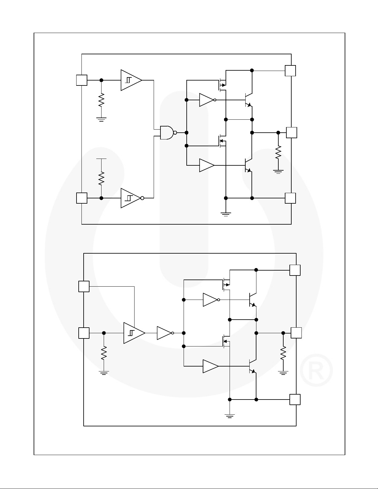
Figure 3. FAN3111C Simplified Block Diagram
100kΩ
2
GND
1
VDD
4
2
5
OUT
GND
IN+
© 2008 Fairchild Semiconductor Corporation www.fairchildsemi.com
FAN3111 • Rev. 1.0.3 3
3
100kΩ
100kΩ
Figure 4. FAN3111E Simplified Block Diagram

Absolute Maximum Ratings
Stresses exceeding the absolute maximum ratings may damage the device. The device may not function or be
operable above the recommended operating conditions and stressing the parts to these levels is not recommended.
In addition, extended exposure to stresses above the recommended operating conditions may affect device reliability.
The absolute maximum ratings are stress ratings only.
FAN3111 — Single 1A High-Speed, Low-Side Gate Driver
Symbol Parameter Min. Max.
Uni
t
VDD VDD to GND -0.3 20.0 V
VIN Voltage on IN to GND
FAN3111C -0.3 V
FAN3111E -0.3 V
V
Voltage on XREF to GND FAN3111E -0.3 5.5 V
XREF
V
Voltage on OUT to GND -0.3 VDD+0.3 V
OUT
+ 0.3 V
DD
+0.3 V
XREF
TL Lead Soldering Temperature (10 Seconds) +260 ºC
TJ Junction Temperature +150 ºC
T
Storage Temperature -65 +150 ºC
STG
Recommended Operating Conditions
The Recommended Operating Conditions table defines the conditions for actual device operation. Recommended
operating conditions are specified to ensure optimal performance to the datasheet specifications. Fairchild does not
recommend exceeding them or designing to Absolute Maximum Ratings.
Symbol Parameter Min. Max. Unit
VDD Supply Voltage Range 4.5 18.0 V
VIN Input Voltage IN
FAN3111C 0 V
FAN3111E 0 V
V
External Reference Voltage XREF FAN3111E 2.0 5.0 V
XREF
V
DD
V
XREF
TA Operating Ambient Temperature -40 +125 ºC
© 2008 Fairchild Semiconductor Corporation www.fairchildsemi.com
FAN3111 • Rev. 1.0.3 4

FAN3111 — Single 1A High-Speed, Low-Side Gate Driver
Electrical Characteristics
Unless otherwise noted, VDD = 12V, V
device and negative out of the device.
Symbol Parameter Conditions Min. Typ. Max. Unit
Supply
VDD Operating Range 4.5 18.0 V
IDD Static Supply Current Inputs Not Connected 5 10 µA
Inputs (FAN3111C)
V
IN Logic, Low-Voltage Threshold 30 38 %VDD
IL_C
V
IN Logic, High-Voltage Threshold 55 70 %VDD
IH_C
I
IN Current, Low IN from 0 to VDD -1 175 µA
INL
I
IN Current, High IN from 0 to VDD -175 1 µA
INH
V
Input Hysteresis Voltage 17 %VDD
HYS_C
Inputs (FAN3111E)
V
IN Logic, Low-Voltage Threshold 25 30 %V
IL_E
V
IN Logic, High-Voltage Threshold 50 60 %V
IH_E
I
IN Current, Low IN from 0 to V
INL
I
IN Current, High IN from 0 to V
INH
V
Input Hysteresis Voltage 20 %V
HYS_E
Output
I
OUT Current, Mid-Voltage, Sinking
SINK
I
OUT Current, Mid-Voltage, Sourcing
SOURCE
I
OUT Current, Peak, Sinking
PK_SINK
I
PK_SOURCE
tD1, tD2 Output Prop. Delay
Notes:
8. Not tested in production.
9. See Timing diagrams.
OUT Current, Peak, Sourcing
t
Output Rise Time
RISE
t
Output Fall Time
FALL
I
Output Reverse Current Withstand
RVS
(9)
C
(9)
C
(9)
= 3.3V, TJ = -40°C to +125°C. Currents are defined as positive into the
XREF
-1 50 µA
XREF
-50 1 µA
XREF
(8)
OUT at V
C
LOAD
OUT at V
C
LOAD
LOAD
LOAD
LOAD
LOAD
(8)
(8)
C
(8)
C
FAN3111C: 0 - 12V
/2,
DD
= 47nF, f = 1KHz
/2,
DD
= 47nF, f = 1KHz
1.1 A
-0.9 A
= 47nF, f = 1KHz 1.4 A
= 47nF, f = 1KHz -1.4 A
= 470pF 9 18 ns
= 470pF 8 17 ns
,
IN
1V/ns Slew Rate
15 30 ns
FAN3111E: 0 - 3.3VIN,
1V/ns Slew Rate
(8)
250 mA
XREF
XREF
XREF
© 2008 Fairchild Semiconductor Corporation www.fairchildsemi.com
FAN3111 • Rev. 1.0.3 5

Timing Diagrams
90%
Output
10%
V
IN+
INH
V
INL
FAN3111 — Single 1A High-Speed, Low-Side Gate Driver
90%
Output
10%
V
IN -
t
D1
t
D2
INH
V
INL
t
D1
t
D2
t
RISE
t
FALL
t
FALL
t
RISE
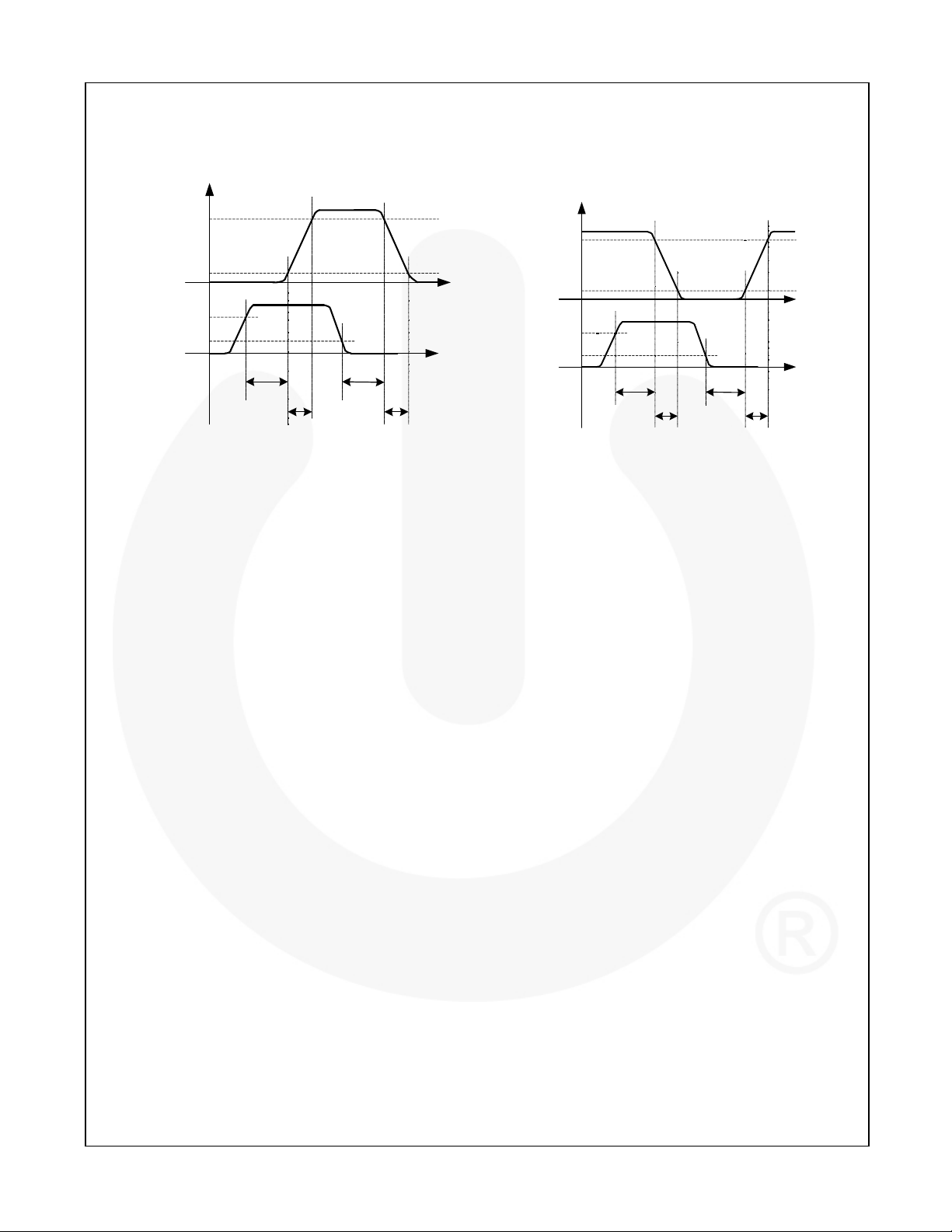
Figure 5. Non-Inverting Waveforms Figure 6. Inverting Waveforms
© 2008 Fairchild Semiconductor Corporation www.fairchildsemi.com
FAN3111 • Rev. 1.0.3 6
 Loading...