FAN3100
Single 2A High-Speed, Low-Side Gate Driver
Features
3A Peak Sink/Source at V
= 12V
DD
4.5 to 18V Operating Range
2.5A Sink / 1.8A Source at V
OUT
= 6V
Dual-Logic Inputs Allow Configuration as
Non-Inverting or Inverting with Enable Function
Internal Resistors Turn Driver Off If No Inputs
13ns Typical Rise Time and 9ns Typical Fall-Time
with 1nF Load
Choice of TTL or CMOS Input Thresholds
MillerDrive™ Technology
Typical Propagation Delay Time Under 20ns with
Input Falling or Rising
6-Lead 2x2mm MLP or 5-Pin SOT23 Packages
Rated from –40°C to 125°C Ambient
Applications
Switch-Mode Power Supplies
High-Efficiency MOSFET Switching
Synchronous Rectifier Circuits
DC-to-DC Converters
Motor Control
Description
The FAN3100 2A gate driver is designed to drive an Nchannel enhancement-mode MOSFET in low-side
switching applications by providing high peak current
pulses during the short switching intervals. The driver is
available with either TTL (FAN3100T) or CMOS
(FAN3100C) input thresholds. Internal circuitry provides
an under-voltage lockout function by holding the output
low until the supply voltage is within the operating range.
The FAN3100 delivers fast MOSFET switching
performance, which helps maximize efficiency in highfrequency power converter designs.
FAN3100 drivers incorporate MillerDrive™ architecture
for the final output stage. This bipolar-MOSFET
combination provides high peak current during the Miller
plateau stage of the MOSFET turn-on / turn-off process
to minimize switching loss, while providing rail-to-rail
voltage swing and reverse current capability.
The FAN3100 also offers dual inputs that can be
configured to operate in non-inverting or inverting mode
and allow implementation of an enable function. If one or
both inputs are left unconnected, internal resistors bias
the inputs such that the output is pulled low to hold the
power MOSFET off.
The FAN3100 is available in a lead-free finish 2x2mm 6lead Molded Leadless Package (MLP), for smallest size
with excellent thermal performance, or industry-standard
5-pin SOT23.
FAN3100 — Single 2A High-Speed, Low-Side Gate Driver
July 2012
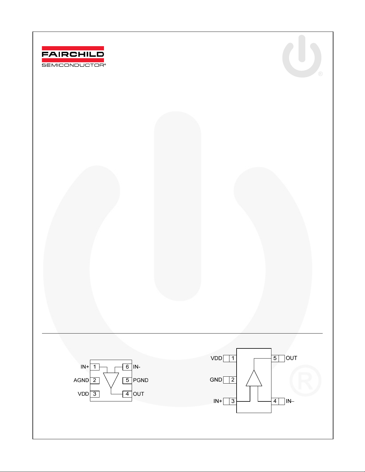
Functional Pin Configurations
Figure 1. 2x2mm 6-Lead MLP (Top View) Figure 2. SOT23-5 (Top View)
© 2007 Fairchild Semiconductor Corporation www.fairchildsemi.com
FAN3100 • Rev. 1.0.4

Ordering Information
FAN3100 — Single 2A High-Speed, Low-Side Gate Driver
Part Number
Input
Threshold
Package Packing Method Quantity / Reel
FAN3100CMPX CMOS 6-Lead 2x2mm MLP Tape & Reel 3000
FAN3100CSX CMOS 5-Pin SOT23 Tape & Reel 3000
FAN3100TMPX TTL 6-Lead 2x2mm MLP Tape & Reel 3000
FAN3100TSX TTL 5-Pin SOT23 Tape & Reel 3000
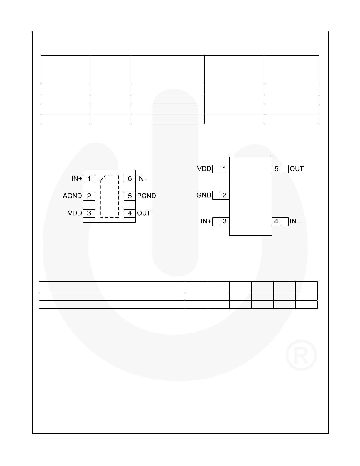
Package Outlines
Figure 3. 2x2mm 6-Lead MLP (Top View) Figure 4. SOT23-5 (Top View)
Thermal Characteristics
Package
6-Lead 2x2mm Molded Leadless Package (MLP) 2.7 133 58 2.8 42 °C/W
SOT23-5 56 99 157 51 5 °C/W
Notes:
1. Estimates derived from thermal simulation; actual values depend on the application.
2. Theta_JL (
thermal pad) that are typically soldered to a PCB.
3. Theta_JT (
held at a uniform temperature by a top-side heatsink.
4. Theta_JA (Θ
The value given is for natural convection with no heatsink using a 2SP2 board, as specified in JEDEC standards JESD51-2,
JESD51-5, and JESD51-7, as appropriate.
5. Psi_JB (
application circuit board reference point for the thermal environment defined in Note 4. For the MLP-6 package, the board
reference is defined as the PCB copper connected to the thermal pad and protruding from either end of the package. For the
SOT23-5 package, the board reference is defined as the PCB copper adjacent to pin 2.
6. Psi_JT (
the center of the top of the package for the thermal environment defined in Note 4.
Θ
): Thermal resistance between the semiconductor junction and the bottom surface of all the leads (including any
JL
Θ
): Thermal resistance between the semiconductor junction and the top surface of the package, assuming it is
JT
): Thermal resistance between junction and ambient, dependent on the PCB design, heat sinking, and airflow.
JA
Ψ
): Thermal characterization parameter providing correlation between semiconductor junction temperature and an
JB
Ψ
): Thermal characterization parameter providing correlation between the semiconductor junction temperature and
JT
(1)
(2)
Θ
JL
Θ
(3)
JT
Θ
JA
(4)
Ψ
JB
(5)
Ψ
(6)
Units
JT
© 2007 Fairchild Semiconductor Corporation www.fairchildsemi.com
FAN3100 • Rev. 1.0.4 2

Pin Definitions
FAN3100 — Single 2A High-Speed, Low-Side Gate Driver
SOT23
Pin #
MLP
Pin #
1 3 VDD
2 AGND
2 GND
3 1 IN+
4 6
5 4 OUT
Pad P1
5 PGND
Name Pin Description
Supply Voltage. Provides power to the IC.
Analog ground for input signals (MLP only). Connect to PGND underneath the IC.
Ground (SOT-23 only). Common ground reference for input and output circuits.
Non-Inverting Input. Connect to VDD to enable output.
Inverting Input. Connect to AGND or PGND to enable output.
IN-
Gate Drive Output: Held low unless required inputs are present and V
threshold.
Thermal Pad (MLP only). Exposed metal on the bottom of the package which is
electrically connected to pin 5.
Power Ground (MLP only). For output drive circuit; separates switching noise from
inputs.
Output Logic
IN+ IN− OUT
(7)
0
0 0
(7)
0
1
1 0 1
1 1
Note:
7. Default input signal if no external connection is made.
(7)
0
(7)
0
is above UVLO
DD
© 2007 Fairchild Semiconductor Corporation www.fairchildsemi.com
FAN3100 • Rev. 1.0.4 3

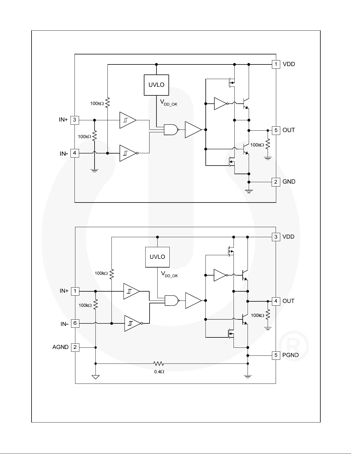
Block Diagrams
FAN3100 — Single 2A High-Speed, Low-Side Gate Driver
Figure 5. Simplified Block Diagram (SOT23 Pin-out)
Figure 6. Simplified Block Diagram (MLP Pin-out)
© 2007 Fairchild Semiconductor Corporation www.fairchildsemi.com
FAN3100 • Rev. 1.0.4 4

Absolute Maximum Ratings
Stresses exceeding the absolute maximum ratings may damage the device. The device may not function or be
operable above the recommended operating conditions and stressing the parts to these levels is not recommended.
In addition, extended exposure to stresses above the recommended operating conditions may affect device reliability.
The absolute maximum ratings are stress ratings only.
Symbol Parameter Min. Max. Unit
VDD VDD to PGND -0.3 20.0 V
VIN Voltage on IN+ and IN- to GND, AGND, or PGND GND - 0.3 VDD + 0.3 V
V
Voltage on OUT to GND, AGND, or PGND GND - 0.3 VDD + 0.3 V
OUT
TL Lead Soldering Temperature (10 seconds) +260 ºC
TJ Junction Temperature -55 +150 ºC
T
Storage Temperature -65 +150 ºC
STG
Recommended Operating Conditions
The Recommended Operating Conditions table defines the conditions for actual device operation. Recommended
operating conditions are specified to ensure optimal performance to the datasheet specifications. Fairchild does not
recommend exceeding them or designing to Absolute Maximum Ratings.
FAN3100 — Single 2A High-Speed, Low-Side Gate Driver
Symbol Parameter Min. Max. Unit
VDD Supply Voltage Range 4.5 18.0 V
VIN Input Voltage IN+, IN- 0 VDD V
TA Operating Ambient Temperature -40 +125 ºC
© 2007 Fairchild Semiconductor Corporation www.fairchildsemi.com
FAN3100 • Rev. 1.0.4 5

FAN3100 — Single 2A High-Speed, Low-Side Gate Driver
Electrical Characteristics
Unless otherwise noted, VDD = 12V, TJ = -40°C to +125°C. Currents are defined as positive into the device and
negative out of the device.
Symbol Parameter Conditions Min. Typ. Max. Unit
Supply
VDD Operating Range 4.5 18.0 V
(8)
IDD
Supply Current
Inputs/EN Not Connected
FAN3100C
FAN3100T 0.5 0.8 mA
VON Turn-On Voltage 3.5 3.9 4.3 V
V
Turn-Off Voltage 3.3 3.7 4.1 V
OFF
Inputs (FAN3100T)
V
IN+, IN- Logic Low Voltage, Maximum 0.8 V
INL_T
V
IN+, IN- Logic High Voltage, Minimum 2.0 V
INH_T
I
Non-inverting Input IN from 0 to VDD -1 175 µA
IN+
I
Inverting Input IN from 0 to VDD -175 1 µA
IN-
V
IN+, IN- Logic Hysteresis Voltage 0.2 0.4 0.8 V
HYS
Inputs (FAN3100C)
V
IN+, IN- Logic Low Voltage 30 %VDD
INL_C
V
IN+, IN- Logic High Voltage 70 %VDD
INH_C
I
IN Current, Low IN from 0 to VDD -1 175 µA
INL
I
IN Current, High IN from 0 to VDD -175 1 µA
INH
V
IN+, IN- Logic Hysteresis Voltage 17 %VDD
HYS_C
Output
OUT at V
I
OUT Current, Mid-Voltage, Sinking
SINK
I
OUT Current, Mid-Voltage, Sourcing
SOURCE
I
OUT Current, Peak, Sinking
PK_SINK
I
PK_SOURCE
OUT Current, Peak, Sourcing
t
Output Rise Time
RISE
t
Output Fall Time
FALL
(10)
C
(10)
C
tD1, tD2 Output Prop. Delay, CMOS Inputs
tD1, tD2 Output Prop. Delay, TTL Inputs
I
Output Reverse Current Withstand
RVS
(9)
C
LOAD
OUT at V
(9)
C
LOAD
(9)
C
(9)
C
(10)
(10)
0 - 5VIN; 1V/ns Slew Rate 9 16 30 ns
(9)
LOAD
LOAD
LOAD
LOAD
0 - 12VIN; 1V/ns Slew Rate 7 15 28 ns
500 mA
Note:
8. Lower supply current due to inactive TTL circuitry.
9. Not tested in production.
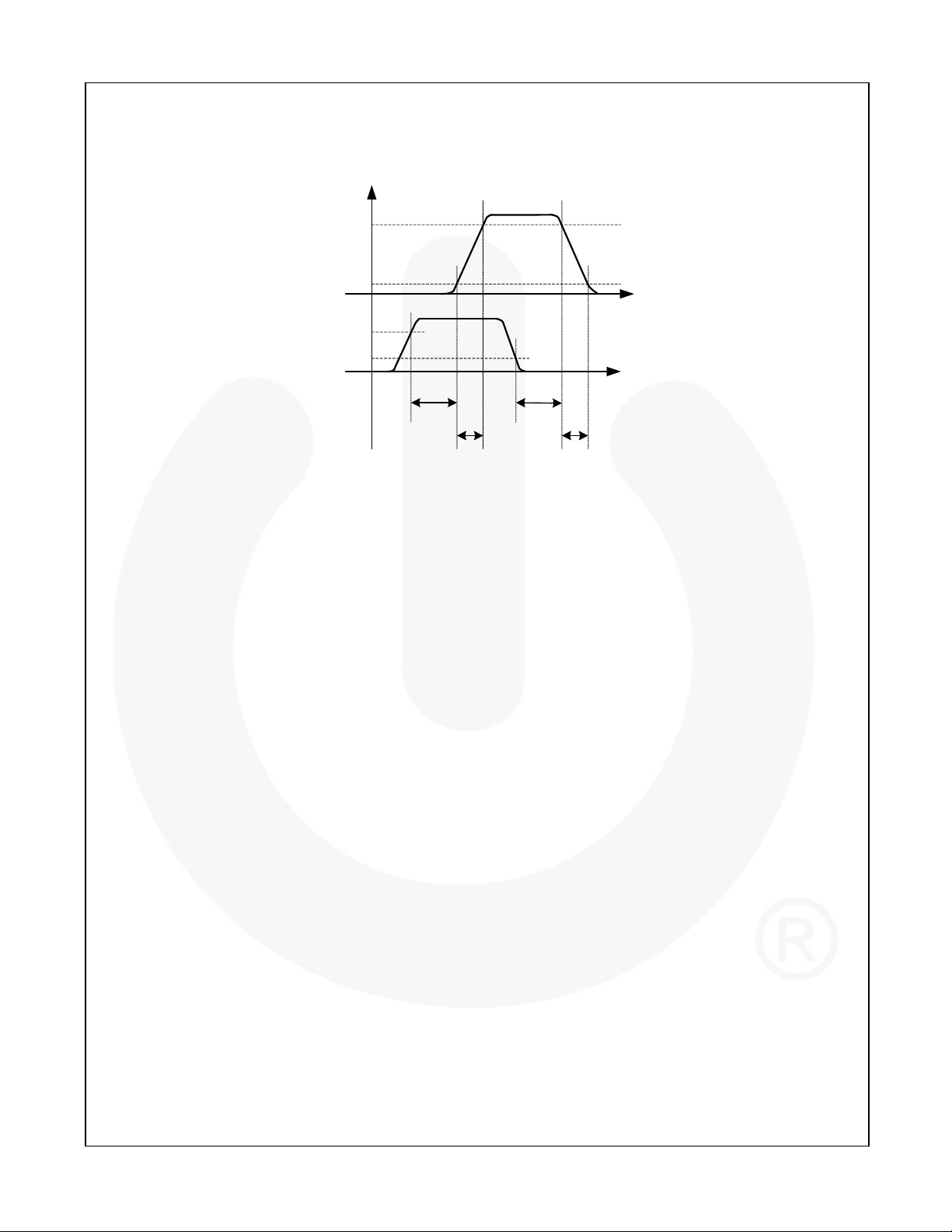
10. See Timing Diagrams of Figure 7 and Figure 8.
0.20 0.35 mA
/2,
DD
= 0.1µF, f = 1kHz
/2,
DD
= 0.1µF, f = 1kHz
2.5 A
-1.8 A
= 0.1µF, f = 1kHz 3 A
= 0.1µF, f = 1kHz -3 A
= 1000pF 13 20 ns
= 1000pF 9 14 ns
© 2007 Fairchild Semiconductor Corporation www.fairchildsemi.com
FAN3100 • Rev. 1.0.4 6

Timing Diagrams
Output
Input
90%
10%
V
INH
V
INL
FAN3100 — Single 2A High-Speed, Low-Side Gate Driver
t
D1
t
RISE
t
D2
t
FALL
Figure 7. Non-Inverting
© 2007 Fairchild Semiconductor Corporation www.fairchildsemi.com
FAN3100 • Rev. 1.0.4 7
 Loading...