January 2013
FAN302HLMY_F117
PWM Controller for Low Standby Power BatteryCharger Applications — mWSaver™ Technology
FAN302HLMY_F117 — mWSaver™ PWM Controller for Low Standby Power Battery-Charger Applications
Features
mWSaver™ Technology Provides Industry’s
Best-in-Class Standby Power
- Ultra Low Power Consumption at No Load
(<10 mW at 230 V
AC
)
- Proprietary 500V High-Voltage JFET Startup
Reduces Startup Resistor Loss
- Low Operation Current in Burst Mode:
350 µA Maximum
Constant-Current (CC) Control without Secondary-
Feedback Circuitry
Fixed PWM Frequency at 85kHz with Frequency
Hopping to Reduce EMI
High-Voltage Startup
Low Operating Current: 3.5 mA
Peak-Current-Mode Control with Slope
Compensation
Cycle-by-Cycle Current Limiting
V
V
V
Over-Voltage Protection (Auto-Restart)
DD
Over-Voltage Protection (Latch Mode)
S
Under-Voltage Lockout (UVLO)
DD
Gate Output Maximum Voltage Clamped at 15 V
Fixed Over-Temperature Protection (Latch Mode)
Available in an 8-Lead SOIC Package
Description
The FAN302HLMY_F117 advanced PWM controller
significantly simplifies isolated power supply design that
requires CC regulation of the output. The output current
is precisely estimated with information in the primary
side of the transformer and controlled with an internal
compensation circuit. This removes the output current
sensing loss and eliminates all external Control Circuitry
(CC). The Green-Mode function, with an extremely low
operating current (200 µA) in Burst Mode, maximizes
the light-load efficiency, enabling conformance to
worldwide Standby Mode efficiency guidelines.
Integrated protections include two-level pulse-by-pulse
current limit, Over-Voltage Protection (OVP), brownout
protection, and Over-Temperature Protection (OTP).
Compared with a conventional approach using an
external control circuit in the secondary side for CC
regulation, the FAN302HLMY_F117 can reduce total
cost, component count, size, and weight; while
simultaneously increasing efficiency, productivity, and
system reliability.
V
O
Maximum
Typical
Minimum
Applications
Battery Chargers for Cellular Phones, Cordless
Phones, PDAs, Digital Cameras, and Power Tools
Replaces Linear Regulators and RCC SMPS
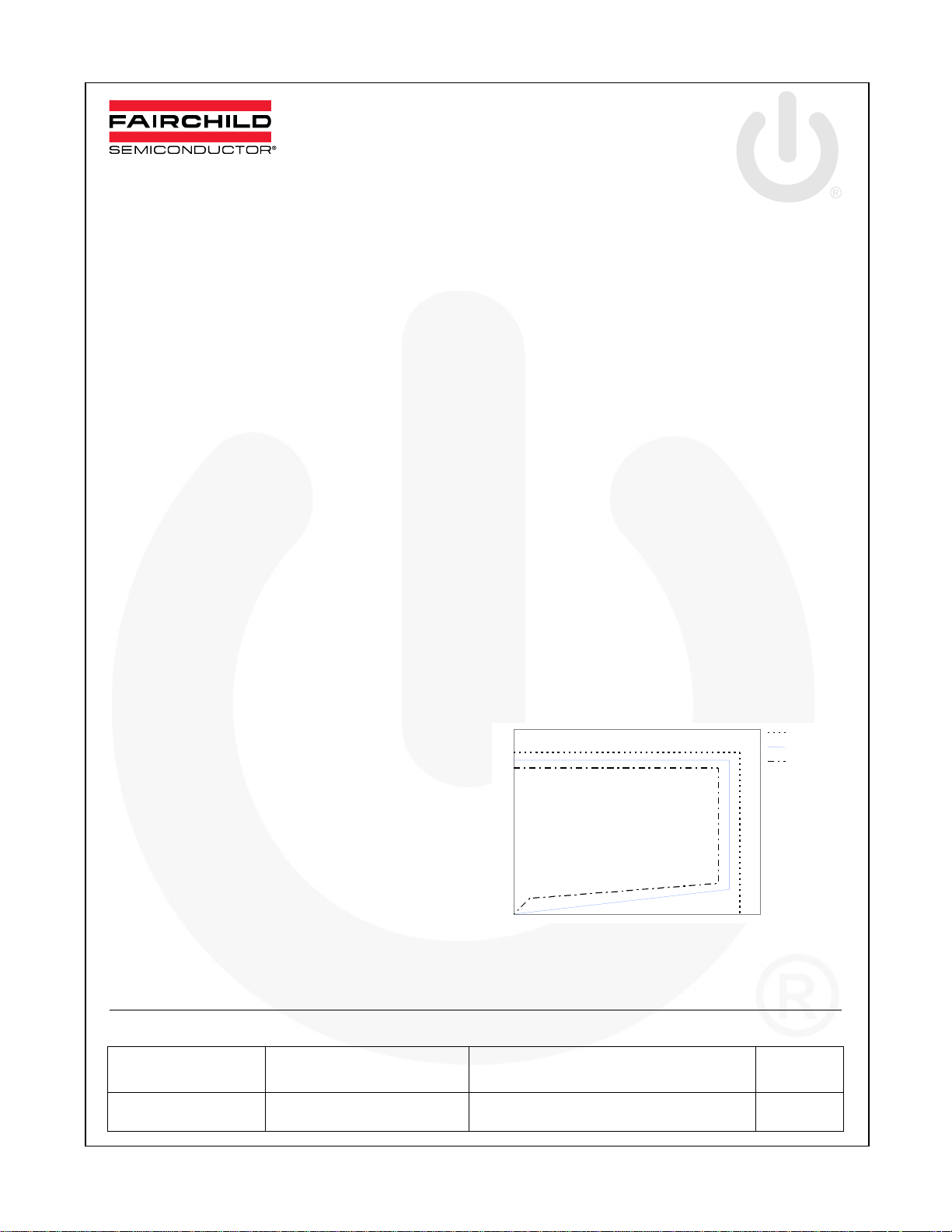
Figure 1. Typical Output V-I Characteristic
I
O
Ordering Information
Part Number
FAN302HLMY_F117
© 2012 Fairchild Semiconductor Corporation www.fairchildsemi.com
FAN302HLMY_F117 • Rev. 1.0.2
Operating
Temperature Range
-40°C to +105°C
Package
8-Lead, Small Outline Package (SOIC),
JEDEC MS-012, .150-Inch Narrow Body
Packing
Method
Tape & Reel
Application Diagram
FAN302HLMY_F117— mWSaver™ PWM Controller for Low Standby Power Battery-Charger Applications
Internal Block Diagram
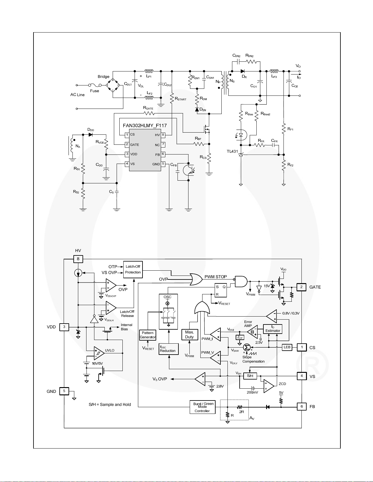
Figure 2. Typical Application
Figure 3. Functional Block Diagram
© 2012 Fairchild Semiconductor Corporation www.fairchildsemi.com
FAN302HLMY_F117 • Rev. 1.0.2 2
Marking Information
FAN302HLMY_F117— mWSaver™ PWM Controller for Low Standby Power Battery-Charger Applications
Pin Configuration
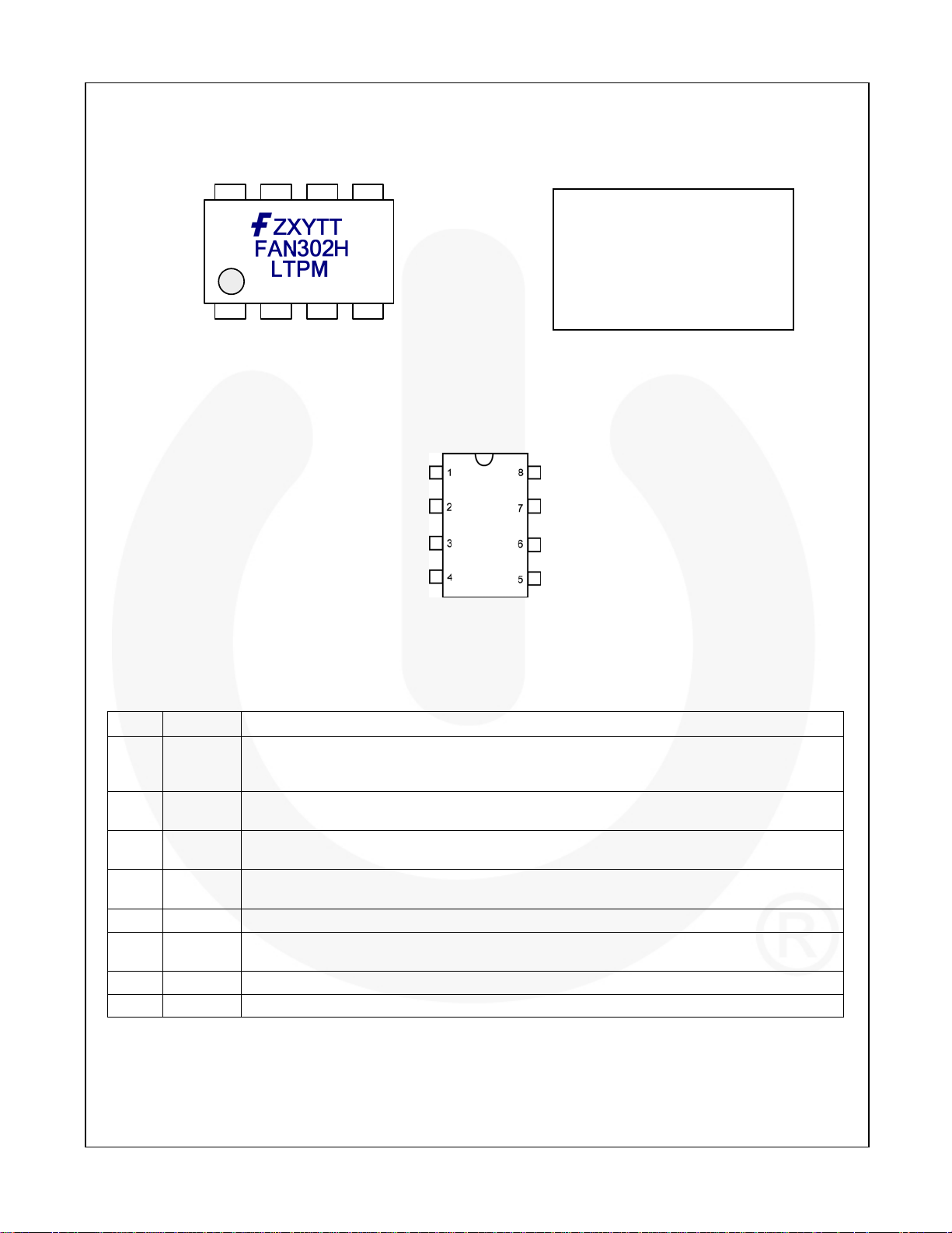
Figure 4.Top Mark
CS
GATE
VDD
VS
Figure 5. Pin Assignments
F- Fairchild Logo
Z: Assembly Plant Code
X: Year Code
Y: Week Code
TT: Die Run Code
T: M=SOIC
P: Y= Green Package
M: Manufacture Flow Code
HV
NC
FB
GND
Pin Definitions
Pin # Name Description
Current Sense. This pin connects a current-sense resistor to sense the MOSFET current for
1 CS
2 GATE
3 VDD
4 VS
5 GND
6 FB
7 NC No Connect
8 HV
Peak-Current-Mode control for output regulation. The current-sense information is also used to
estimate the output current for CC regulation.
PWM Signal Output. This pin has an internal totem-pole output driver to drive the power
MOSFET. It is internally clamped at 15 V.
Power Supply. IC operating current and MOSFET driving current are supplied through this pin.
This pin is typically connected to an external V
Voltage Sense. This pin detects the output voltage information and diode current discharge
time based on the voltage of the auxiliary winding.
Ground
Feedback. Typically, an opto-coupler is connected to this pin to provide feedback information to
the internal PWM comparator. This feedback is used to control the duty cycle in CV regulation.
High Voltage. This pin connects to the DC bus for high-voltage startup.
capacitor.
DD
© 2012 Fairchild Semiconductor Corporation www.fairchildsemi.com
FAN302HLMY_F117 • Rev. 1.0.2 3
FAN302HLMY_F117— mWSaver™ PWM Controller for Low Standby Power Battery-Charger Applications
Absolute Maximum Ratings
Stresses exceeding the Absolute Maximum Ratings may damage the device. The device may not function or be
operable above the recommended operating conditions and stressing the parts to these levels is not recommended.
In addition, extended exposure to stresses above the recommended operating conditions may affect device reliability.
The absolute maximum ratings are stress ratings only.
Symbol Parameter Min. Max. Unit
VHV HV Pin Input Voltage 500 V
V
DC Supply Voltage
VDD
VVS VS Pin Input Voltage -0.3 7.0 V
VCS CS Pin Input Voltage -0.3 7.0 V
VFB FB Pin Input Voltage -0.3 7.0 V
PD
Power Dissipation (TA=25°C)
θJA Thermal Resistance (Junction-to-Air) 150
θJC Thermal Resistance (Junction-to-Case) 39
TJ Operating Junction Temperature -40 +150
T
Storage Temperature Range -55 +150
STG
TL Lead Temperature, (Wave Soldering or IR, 10 Seconds) +260
ESD Electrostatic Discharge Capability
Notes:
1. All voltage values, except differential voltages, are given with respect to GND pin.
2. Stresses beyond those listed under Absolute Maximum Ratings may cause permanent damage to the device.
3. ESD ratings including the HV pin: HBM=400 V, CDM=750 V.
(1,2)
30 V
660 mW
°C/W
°C/W
°C
°C
°C
Human Body Model,
JEDEC:JESD22_A114
(Except HV Pin)
(3)
Charged Device Model,
JEDEC:JESD22_C101
(Except HV Pin)
(3)
5000
V
1500
© 2012 Fairchild Semiconductor Corporation www.fairchildsemi.com
FAN302HLMY_F117 • Rev. 1.0.2 4
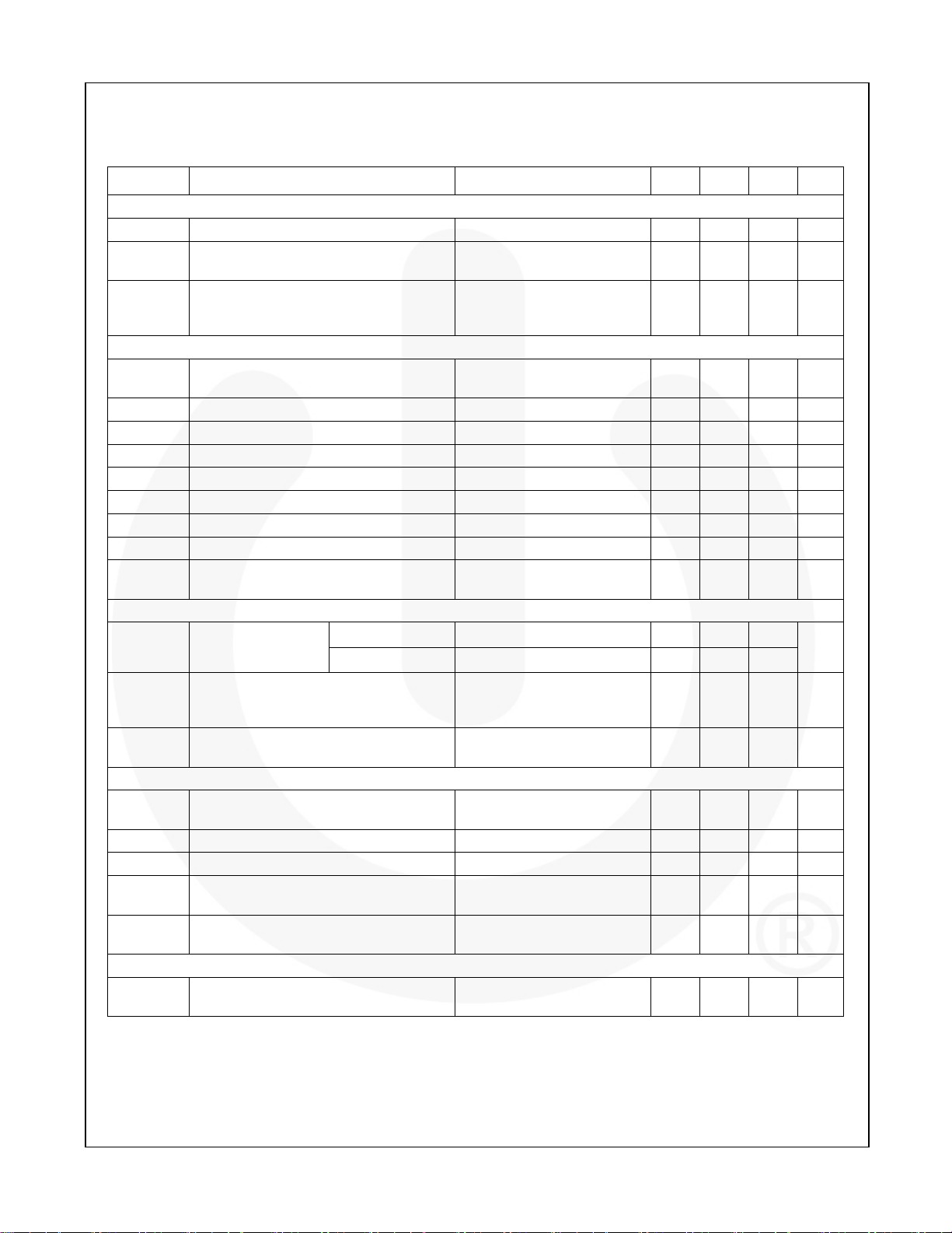
Electrical Characteristics
VDD=15 V and TA=25°C unless noted.
Symbol Parameter Condition Min. Typ. Max. Unit
HV Section
V
Minimum Startup Voltage on HV Pin 50 V
HV-MIN
V
=100 V, VDD=0 V,
IHV Supply Current Drawn from HV Pin
I
Leakage Current Drawn from HV Pin
HV-LC
VDD Section
VOP Continuous Operation Voltage
V
Turn-On Threshold Voltage VDD Rising 15 16 17 V
DD-ON
V
Turn-Off Threshold Voltage VDD Falling 4.7 5.0 5.3 V
DD-OFF
V
Threshold Voltage for Latch-Off Release VDD Falling 2.5 V
DD-LH
I
Startup Current VDD=V
DD-ST
I
Operating Supply Current VDD=18 V, f=f
DD-OP
I
DD-BURST
V
t
D-VDDOVP
Burst-Mode Operating Supply Current VDD=8 V, C
VDD Over-Voltage Protection Level 25.0 26.5 28.0 V
DD-OVP
VDD Over-Voltage Protection Debounce
Time
Oscillator Section
Center Frequency VCS=5 V, VS=2.5 V, VFB=5 V 82 85 88
f
Frequency
OSC
Hopping Range
Minimum Frequency for Continuous
f
OSC-CM-MIN
f
OSC-CCM
Conduction Mode (CCM) Prevention
(4)
Circuit
Minimum Frequency in Constant Current
(CC) Regulation
Feedback Input Section
AV
Internal Voltage Scale-Down Ratio of FB
(5)
Pin
ZFB FB Pin Input Impedance 38 42 44 k
V
FB Pin Pull-Up Voltage FB Pin Open 5.3 V
FB-OPEN
V
FB-L
V
FB-H
FB Threshold to Disable Gate Drive in
Burst Mode
FB Threshold to Enable Gate Drive in
Burst Mode
Over-Temperature Protection Section
T
OTP
Threshold for Over-Temperature
Protection (OVP)
HV
Controller Off
0.8 1.5 5.0 mA
VHV=500 V, VDD=15 V
(Controller On with Auxiliary
0.8 3.0 A
Supply)
Limited by V
Protection (OVP)
DD-ON
Over-Voltage
DD
25 V
– 0.16 V 400 450 A
, C
OSC
=1 nF 200 350 A
GATE
=1 nF 3.5 4.0 mA
GATE
f=85 kHz 100 180 s
±3
13 18 23 kHz
VCS=5 V, VS=0 V 23 26 29 kHz
1/3.5 1/3.0 1/2.5 V/V
VFB Falling,VCS=5 V, VS=0 V 1.2 1.4 1.6 V
VFB Rising,VCS=5 V, V
=0 V 1.3 1.5 1.7 V
S
+130 +140 +150
FAN302HLMY_F117— mWSaver™ PWM Controller for Low Standby Power Battery-Charger Applications
kHz
°C
Continued on the following page…
© 2012 Fairchild Semiconductor Corporation www.fairchildsemi.com
FAN302HLMY_F117 • Rev. 1.0.2 5
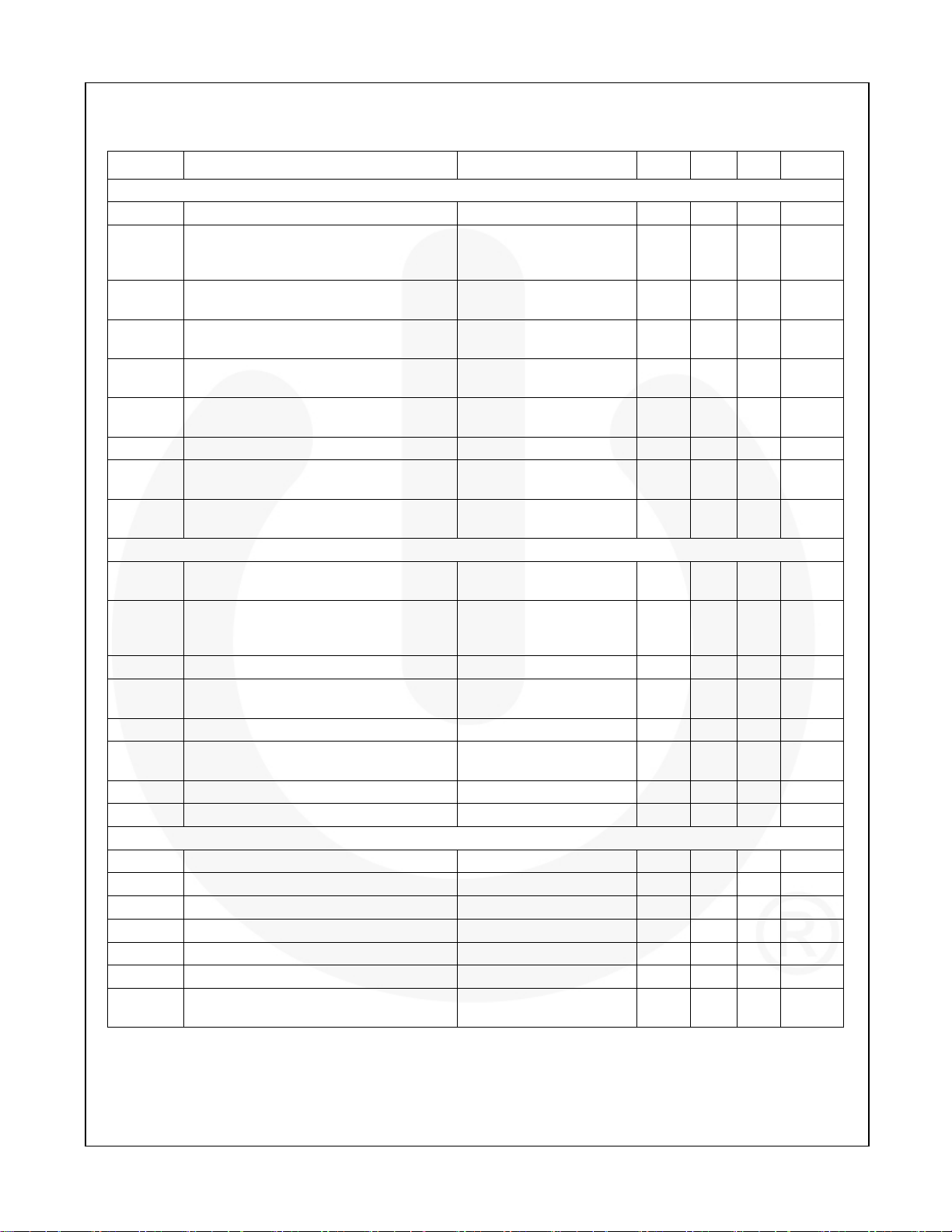
FAN302HLMY_F117— mWSaver™ PWM Controller for Low Standby Power Battery-Charger Applications
Electrical Characteristics (Continued)
VDD=15 V and TA=25°C unless noted.
Symbol Parameter Condition Min. Typ. Max. Unit
Voltage-Sense Section
ITC Bias Current VCS=5 V 8.75 10.00 11.25 A
VS Sampling Voltage to Switch to the
V
VS-CM-MIN
V
VS-CM-MAX
V
SN-CC
V
SG-CC
S
G-CC
V
VS-OFFSET
V
VS-OVP
t
VS-OVP
Current-Sense Section
VVR
V
CCR
V
STH
V
STH-VA
tPD GATE Output Turn-Off Delay 100 150 ns
t
MIN
t
LEB
V
SLOPE
GATE Section
D
MAX
V
GATE-L
V
GATE-H
V
GATE-H
V
GATE-
CLAMP
Notes:
4. f
5. A
6. Guaranteed by design; not production tested.
Second Pulse-by-Pulse Current Limit in
Power Limit Mode
VS Sampling Voltage to Switch Back to the
(6)
Normal Pulse-by-Pulse Current Limit
V
Sampling Voltage to Start Frequency
S
Decreasing in CC Mode
Vs Sampling Voltage to End Frequency
Decreasing in CC Mode
Frequency Decreasing Slope of CC
Regulation
ZCD Comparator Internal Offset Voltage
Output Over-Voltage Protection with V
Sampling Voltage
Output Over-Voltage Protection Debounce
Time
Internal Reference Voltage for CC
Regulation
0.55 V
0.75 V
(6)
V
=5 V, fS1=f
CS
V
=5 V, fS2=f
CS
+2 kHz
S
= (fS1-fS2) / (V
G-CC
V
)
SG-CC
(6)
200 mV
S
2.70 2.80 2.85 V
f
=85 kHz 8 cycles
OSC
-2 kHz 2.05 2.15 2.25 V
OSC
OSC-CCM
SN-CC
0.45 0.70 0.95 V
30 38 46
2.475 2.500 2.525 V
Variation Test Voltage on CS Pin for CC
Output (Non-Inverting Input of Error
V
=0.47 V 2.405 2.430 2.455 V
CS
Amplifier for CC Regulation)
Normal Current Limit Threshold Voltage 0.8 V
Second Current Limit Threshold Voltage,
Power Limit Mode (V
S<VVS-CM-MAX
Minimum On Time
Leading-Edge Blanking Time
Slope Compensation
(6)
Maximum Duty Cycle 0.3 V
)
(6)
100 150 200 ns
=0.3 V 0.30 V
V
VS
V
=5 V, VVS=2.5 V,
CS
=5 V (Test Mode)
V
FB
430 530 630 ns
Maximum Duty Cycle 64 67 70 %
Output Voltage Low VDD=25 V, IO=10 mA 0 1.5 V
Output Voltage High VDD=8 V, IO=1 mA 5 8 V
Output Voltage High VDD=5.5 V, IO=1 mA 4.0 5.5 V
tr Rising Time VDD=15 V, C
tf Falling Time VDD=15 V, C
Gate Output Clamping Voltage V
OSC-CM-MIN
is a scale-down ratio of the internal voltage divider of the FB pin.
V
occurs when the power unit enters CCM operation.
=25 V 13 15 17 V
DD
=1 nF 100 140 180 ns
GATE
=1 nF 30 50 70 ns
GATE
kHz/V
© 2012 Fairchild Semiconductor Corporation www.fairchildsemi.com
FAN302HLMY_F117 • Rev. 1.0.2 6
