

Page 1

User Guide for
FEBFAN302HL_CH442v1
Evaluation Board
FAN302HL 5V / 1A PSR Mobile Phone
Battery Charger
Featured Fairchild Product:
FAN302HL
Direct questions or comments
about this Evaluation Board to:
“Worldwide Direct Support”
Fairchild Semiconductor.com
© 2011 Fairchild Semiconductor Corporation 1 FEBFAN302HL_CH442v1 • Rev. 1.0.0
Page 2

Table of Contents
1. General Introduction ................................................................................................................. 3
1.1. General Specification ...................................................................................................... 3
2. Function Check Report ............................................................................................................. 3
2.1. Input Current ................................................................................................................... 4
2.2. Input Wattage at No-load Condition ............................................................................... 4
2.3. Startup Time.................................................................................................................... 6
2.4. DC Output Rising Time .................................................................................................. 7
2.5. Line and Load Regulation ............................................................................................... 9
2.6. Efficiency ........................................................................................................................ 9
2.7. Output Ripple and Noise ............................................................................................... 10
2.8. Step Response ............................................................................................................... 12
2.9. Over-Power Protection .................................................................................................. 13
2.10. Hold-up Time ................................................................................................................ 13
2.11. Short-Circuit Protection ................................................................................................ 15
2.12. Brownout Test ............................................................................................................... 16
2.13. VDD Voltage Level ........................................................................................................ 16
2.14. Voltage Stress on MOSFET and Rectifiers .................................................................. 20
2.15. Constant Voltage (CV) and Constant Current (CC) Curves ......................................... 21
2.16. VS OVP Test ................................................................................................................. 22
2.17. Over-Temperature Protection Test (OTP) .................................................................... 23
2.18. EMI Test ....................................................................................................................... 24
2.19. Surge Test ..................................................................................................................... 25
2.20. ESD Test ....................................................................................................................... 25
3. Photographs............................................................................................................................. 26
4. Schematic ................................................................................................................................ 27
5. PCB Layout ............................................................................................................................. 28
6. Bill of Materials ...................................................................................................................... 29
7. Transformer Specification ...................................................................................................... 30
7.1. Specification Approval ................................................................................................. 30
8. Revision History ..................................................................................................................... 34
© 2011 Fairchild Semiconductor Corporation 2 FEBFAN302HL_CH442v1 • Rev. 1.0.0
Page 3
1. General Introduction
This document describes a 5W power supply using a FAN302HL device. This power
supply is targeted for mobile phone battery chargers with a 10mW solution and requiring
high efficiency.
To get the standby power consumption lower than 10mW at 230VAC, the FAN302HL has
functions to enhance the standby power consumption, including proprietary Burst Mode
with lower operation current under light-load conditions and built-in HV startup circuitry
in the IC side to reduce startup resistor power loss.
Using FAN302HL, a charger can be implemented with the few external components and
minimized cost.
1.1. General Specification
Specification Min. Normal Max. Units
Input
Voltage 90 264 V
Frequency 47 63 Hz
Output
Output Voltage 1 4.75 5.00 5.25 V
Output Current 1 1.0 1.2 1.4 A
RMS
Total Output Power
Full-Load Output Power 4.75 6.00 7.35 W
2. Function Check Report
Test Model
Test Date
Test Temperature
Test Equipment
Test Items
FEBFAN302HL_CH442v1
March 2011
Ambient
AC source: 6800 AC POWER SOURCE
Electronic Load: Chroma 63030 and 63102
Power Meter: WT210
Oscilloscope: LeCory 24Xs-A
1. Input current
2. Input wattage at no-load condition
3. Startup time
4. DC-output rising time
5. Line and load regulation
6. Efficiency
7. Output ripple and noise
8. Step response
9. Over power protection
10. Hold-up time
11. Short-circuit protection
12. Brownout test
13. V
voltage level
DD
© 2011 Fairchild Semiconductor Corporation 3 FEBFAN302HL_CH442v1 • Rev. 1.0.0
Page 4
2.1. Input Current
2.1.1. Test Condition
Measure the AC input current at maximum loading.
2.1.2. Test Result
Input Voltage Input Current (mA) Specification
90V / 60Hz 120.20
264V / 50Hz 51.57
14. Voltage stress on MOSFET and rectifiers
15. Constant voltage (CV) and constant current (CC) curve
16. VS OVP test
17. OTP test
18. EMI test
19. Surge test
20. ESD test
2.2. Input Wattage at No-load Condition
2.2.1. Test Condition
Measure the input wattage and output voltage at no load.
2.2.2. Test Result
Input Voltage Input Wattage (mW) Output Voltage (V) Specification
90V / 60Hz 6.3 5.116
115V / 60Hz 6.5 5.116
230V / 50Hz 7.3 5.116
264V / 50Hz 9.0 5.116
<10mW
© 2011 Fairchild Semiconductor Corporation 4 FEBFAN302HL_CH442v1 • Rev. 1.0.0
Page 5
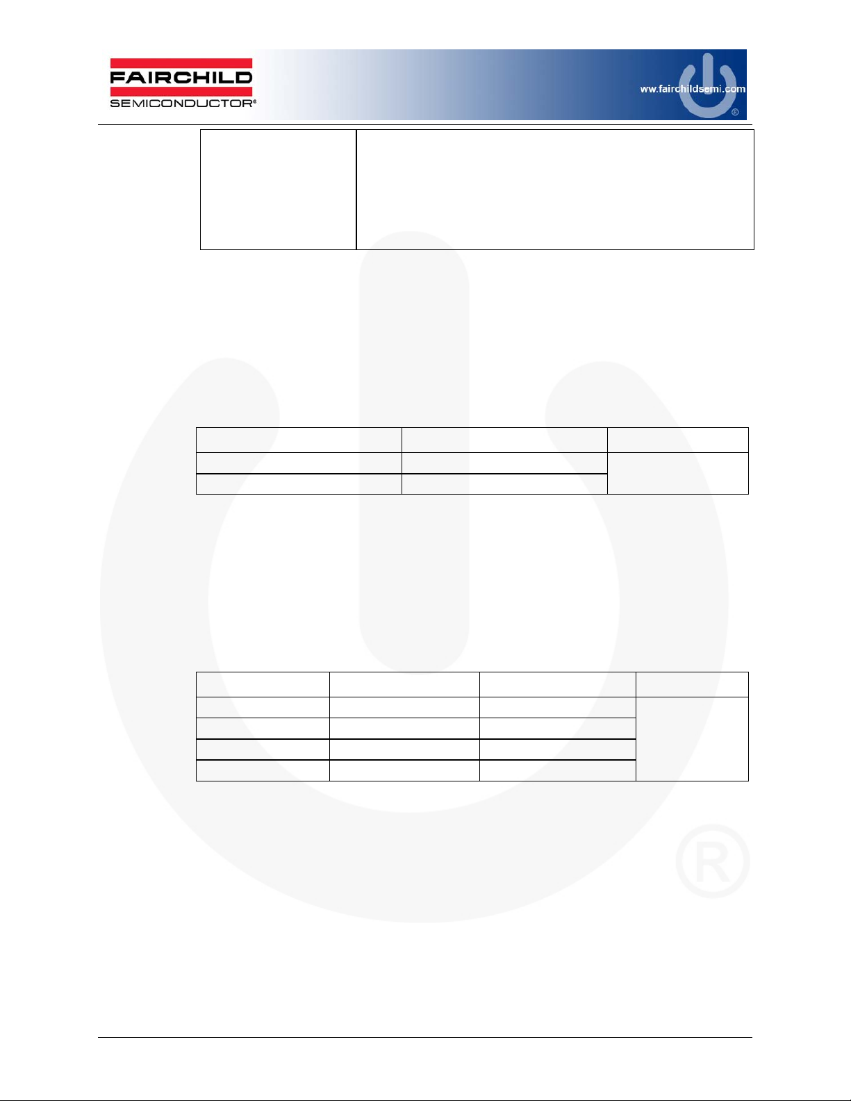
2.2.3. Measured Waveforms
Figure 1. 90V / 60Hz at No Load
Ch1: VFB
Ch2: V
VS
Ch3: V
DD
Ch1: VFB
Ch2: V
VS
Ch3: V
DD
Figure 2. 264V / 50Hz at No Load
© 2011 Fairchild Semiconductor Corporation 5 FEBFAN302HL_CH442v1 • Rev. 1.0.0
Page 6
2.3. Startup Time
2.3.1. Test Condition
Set output at maximum loading. Measure the interval between AC plug-in and stable output.
2.3.2. Test Result
Input Voltage Startup Time (ms) Specification
90V / 60Hz 249
264V / 50Hz 236
2.3.3. Measured Waveforms
<3s
Ch1: V
Ch4: VO
AC
Figure 3. 90V / 60Hz at Maximum Load
Ch1: V
Ch4: V
Figure 4. 264V / 50Hz at Maximum Load
© 2011 Fairchild Semiconductor Corporation 6 FEBFAN302HL_CH442v1 • Rev. 1.0.0
AC
O
Page 7
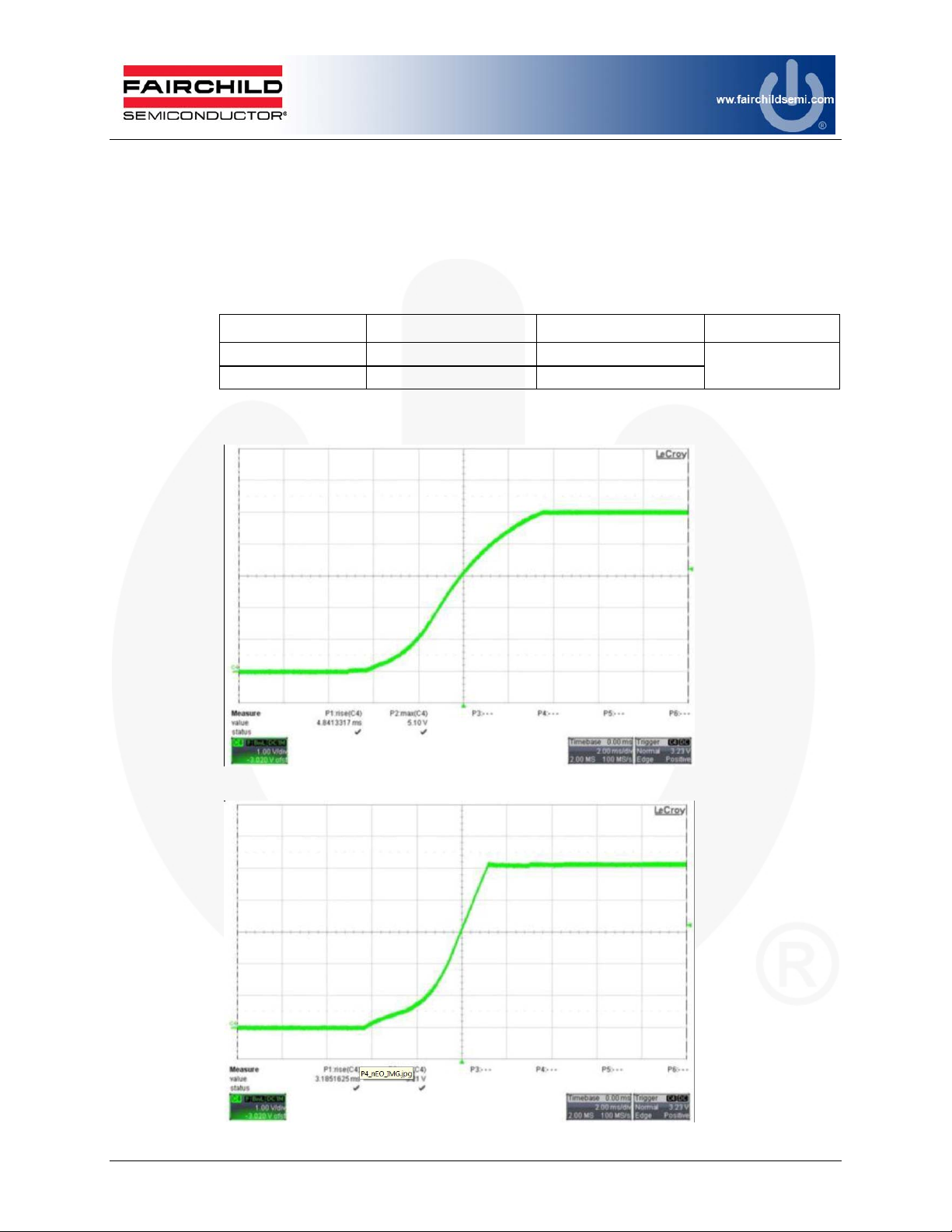
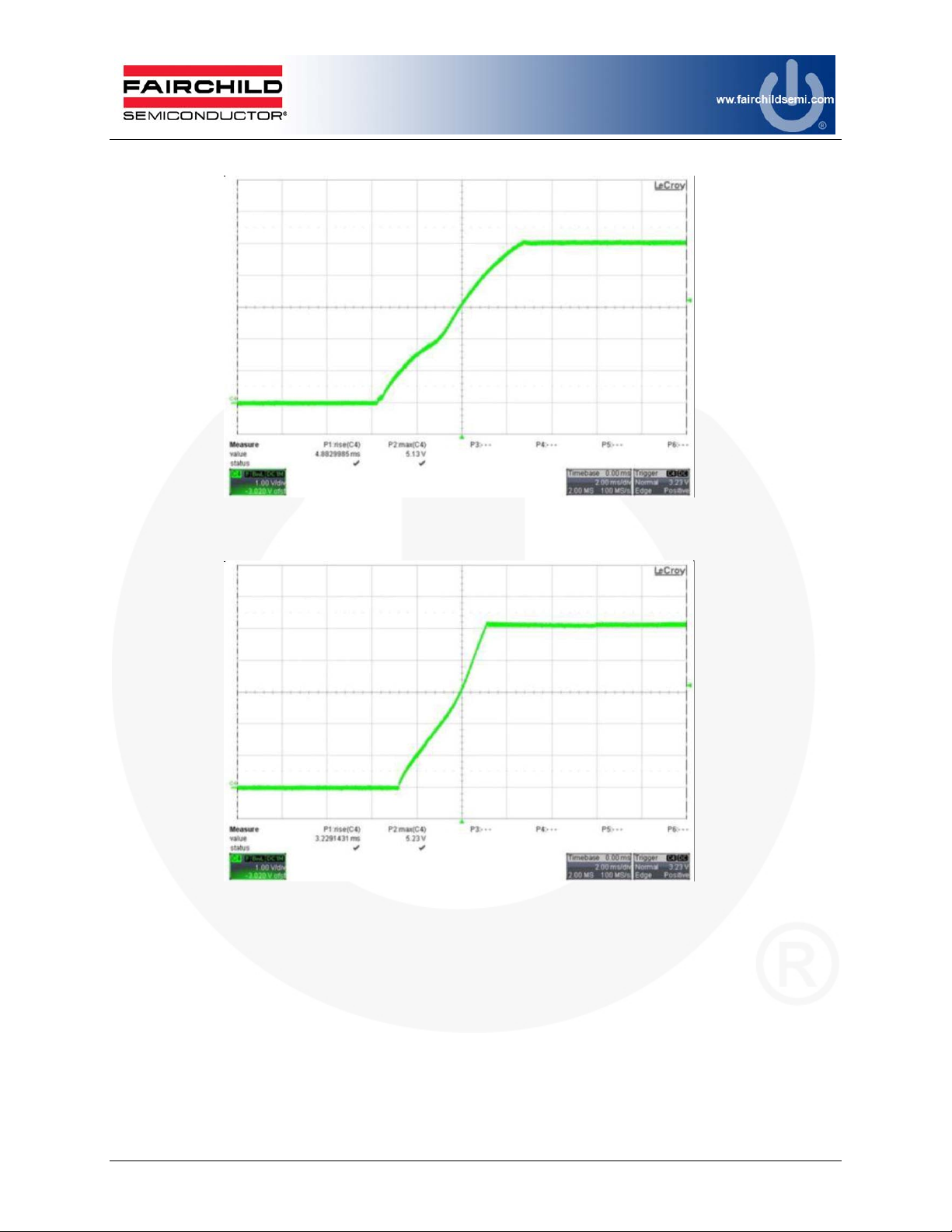
2.4. DC Output Rising Time
2.4.1. Test Condition
Set output at maximum loading and no loading. Measure the time interval between 10%
and 90% output during startup.
2.4.2. Test Result
Input Voltage Maximum Load (ms) No Load (ms) Specification
90V / 60Hz 4.841 3.185
264V / 50Hz 4.882 3.229
2.4.3. Measured Waveforms
<20ms
Figure 5. 90V / 60Hz at Maximum Load
Ch4: V
Ch4: V
O
O
Figure 6. 90V / 60Hz at No Load
© 2011 Fairchild Semiconductor Corporation 7 FEBFAN302HL_CH442v1 • Rev. 1.0.0
Page 8
Ch4: V
O
Figure 7. 264V / 50Hz at Maximum Load
Ch4: V
O
Figure 8. 264V / 50Hz at No Load
© 2011 Fairchild Semiconductor Corporation 8 FEBFAN302HL_CH442v1 • Rev. 1.0.0
Page 9
2.5. Line and Load Regulation
2.5.1. Test Condition
Measure line and load regulation as shown in the table below.
2.5.2. Test Result
Input Voltage
90V / 60Hz 4.990 5.116 2.46
115V / 60Hz 4.994 5.116 2.38
132V / 60Hz 4.998 5.116 2.31
180V / 50Hz 5.006 5.112 2.07
230V / 50Hz 5.018 5.112 1.84
264V / 50Hz 5.022 5.112 1.76
Line Regulation(%) 0.64 0.078
2.6. Efficiency
2.6.1. Test Condition
Measure input wattage and output wattage at maximum load.
2.6.2. Test Result
Input Voltage Input Wattage (W)
90V / 60Hz 6.938 4.980 71.78
115V / 60Hz 6.808 4.990 73.30
132V / 60Hz 6.748 4.994 74.01
180V / 50Hz 6.719 5.006 74.51
230V / 50Hz 6.743 5.016 74.39
264V / 50Hz 6.797 5.024 73.91
Output V at
Max. Load (V)
Output V at
Min. Load (V)
Load
Regulation (%) Specification
Output
Wattage (W) Efficiency (%) Specification
2.6.3. Average Efficiency Test Result
Efficiency(%)
Input
Voltage 25% Load 50% Load 75% Load 100% Load Avg. Spec.
115V / 60Hz 76.06% 75.34% 75.45% 73.30% 74.79%
230V / 50Hz 72.91% 73.52% 74.28% 74.39% 73.78%
Avg>68.17%
© 2011 Fairchild Semiconductor Corporation 9 FEBFAN302HL_CH442v1 • Rev. 1.0.0
Page 10
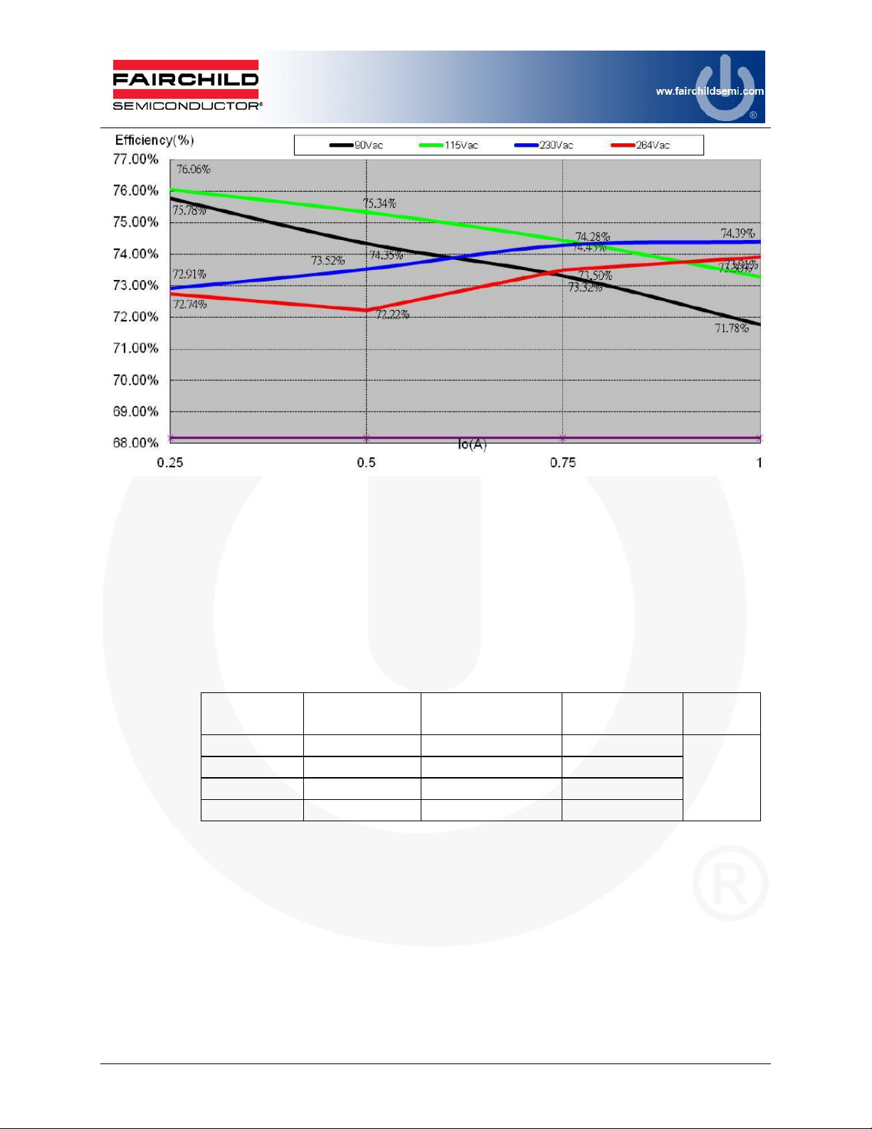
Figure 9. Efficiency Chart
2.7. Output Ripple and Noise
2.7.1. Test Condition
Ripple and noise are measured using a 20MHz bandwidth-limited oscilloscope with a
10μF capacitor paralleled with a high-frequency 0.1μF capacitor across each output.
2.7.2. Test Result
Input Voltage Max. Load (mV)
90V / 60Hz 38 56 15
115V / 60Hz 34 52 16
230V / 50Hz 33 57 25
264V / 50Hz 32 65 22
Before Leaving
Burst Mode (mV) Min. Load (mV) Spec.
<150mV
© 2011 Fairchild Semiconductor Corporation 10 FEBFAN302HL_CH442v1 • Rev. 1.0.0
Page 11
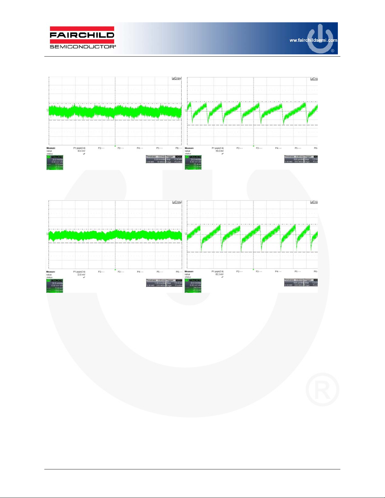
2.7.3. Measured Waveforms
Ch4: V
O
Figure 10. 90V / 60Hz at Maximum Load AC and Burst Ripple
Figure 11. 264V / 50Hz at Maximum Load AC and Burst Ripple
Ch4: V
O
© 2011 Fairchild Semiconductor Corporation 11 FEBFAN302HL_CH442v1 • Rev. 1.0.0
Page 12

2.8. Step Response
2.8.1. Test Condition
Dynamic loading (20%–80%) of the full load, 5ms duty cycle, 2.5A/μs rise/fall time).
2.8.2. Test Result
Input Voltage Overshoot (mV) Undershoot (mV) Specification
115V / 60Hz 105.6 112.0
230V / 50Hz 93.6 86.4
2.8.3. Measured Waveforms
Figure 12. 115V / 60Hz at Step Response
Ch4: V
Ch4: V
O
O
Figure 13. 230V / 50Hz at Step Response
© 2011 Fairchild Semiconductor Corporation 12 FEBFAN302HL_CH442v1 • Rev. 1.0.0
Page 13

2.9. Over-Power Protection
2.9.1. Test Condition
Increase output loading gradually. Measure the output maximum power.
2.9.2. Test Result
Input Voltage Output Power (W) Specification
90V / 60Hz 6.00 (4.932V / 1.216A)
115V / 60Hz 6.05 (4.952V / 1.224A)
230V / 50Hz 6.38 (4.958V / 1.290A)
264V / 50Hz 6.40 (4.976V / 1.293A)
2.10. Hold-up Time
2.10.1. Test Condition
Set output at maximum load. Measure the time interval between AC off and output
voltage falling to the lower limit of the rated value. The AC waveform should be off at
zero degrees.
2.10.2. Test Result
Input Voltage Hold-up Time (ms) Specification
90V / 60Hz 11.84
115V / 60Hz 26.06
230V / 50Hz 108.7
264V / 50Hz 149.5
© 2011 Fairchild Semiconductor Corporation 13 FEBFAN302HL_CH442v1 • Rev. 1.0.0
Page 14

2.10.3. Measured Waveforms
Figure 14. 90V / 60Hz at Maximum Load
Ch1: VAC
Ch4: V
O
Ch1: V
Ch4: V
AC
O
Figure 15. 264V / 50Hz at Maximum Load
© 2011 Fairchild Semiconductor Corporation 14 FEBFAN302HL_CH442v1 • Rev. 1.0.0
Page 15

2.11. Short-Circuit Protection
2.11.1. Test Condition
Short the output of the power supply. The power supply should enter “Hiccup” Mode
protection with less than 2W input voltage.
2.11.2. Test Result
Input Voltage
Input Wattage at
Maximum Loading (W)
Input Wattage at
Minimum Loading (W)
90V / 60Hz 0.468 0.465
264V / 50Hz 0.93 0.95
2.11.3. Measured Waveforms
Figure 16. 90V / 60Hz at Maximum Load Short
Ch2: V
Ch3: V
Ch4: V
Specification
<2W
sense
DD
O
sense
DD
O
Ch1: V
Ch3: V
Ch4: V
Figure 17. 264V / 60Hz at Maximum Load
© 2011 Fairchild Semiconductor Corporation 15 FEBFAN302HL_CH442v1 • Rev. 1.0.0
Page 16

2.12. Brownout Test
2.12.1. Test Condition
Set output at maximum loading. Decrease input voltage with 5V
step. Record input
AC
wattage and output voltage. After the output is off, increase the AC voltage gradually and
record the recovery voltage.
2.12.2. Test Result
Input Voltage Input Wattage (W) Output Voltage (V)
90V / 60Hz 6.936 4.988
85V / 60Hz 6.962 4.978
80V / 60Hz 7.015 4.976
75V / 60Hz 7.076 4.972
70V / 60Hz 7.174 4.970
65V / 60Hz 7.290 4.966
60V / 60Hz 7.476 4.956
55V / 60Hz 7.413 4.870
50V / 60Hz 7.027 4.666
45V / 60Hz 6.501 4.420
40V / 60Hz 5.793 4.112
35V / 60Hz 4.677 3.642
30V / 60Hz 3.744 3.172
25V / 60Hz 0 0
Recovery Voltage Input Wattage (W) Output Voltage (V)
53V / 60Hz 7.331 4.822 / 0.967A
70V / 60Hz 7.162 4.974 / 1.00A
2.13. VDD Voltage Level
2.13.1. Test Result
90V / 60Hz 7.110 8.819 8.829 16.30
264V / 50Hz 7.830 8.772 8.826 16.10
Min. Load (V) Max. Load (V) Near OPP (V)
© 2011 Fairchild Semiconductor Corporation 16 FEBFAN302HL_CH442v1 • Rev. 1.0.0
Output SC
(Max. Value) (V)
Spec.
<24V
Page 17

2.13.2. Measured Waveforms
Ch2: VCS
Ch3: V
DD
Figure 18. 90V / 60Hz at No Load
Ch2: VCS
DD
Ch3: V
Figure 19. 90V / 60Hz at Maximum Load
© 2011 Fairchild Semiconductor Corporation 17 FEBFAN302HL_CH442v1 • Rev. 1.0.0
Page 18

Ch2: VCS
DD
Ch3: V
Figure 20. 90V / 60Hz at Short Circuit
Ch2: VCS
DD
Ch3: V
Figure 21. 264V / 50Hz at No Load
© 2011 Fairchild Semiconductor Corporation 18 FEBFAN302HL_CH442v1 • Rev. 1.0.0
Page 19

Ch2: VCS
DD
Ch3: V
Figure 22. 264V / 50Hz at Maximum Load
Ch2: V
CS
Ch3: VDD
Figure 23. 264V / 50Hz at Short Circuit
© 2011 Fairchild Semiconductor Corporation 19 FEBFAN302HL_CH442v1 • Rev. 1.0.0
Page 20

2.14. Voltage Stress on MOSFET and Rectifiers
2.14.1. Test Condition
Measure the voltage stress on MOSFET and secondary rectifiers under conditions
specified in Table 2.
2.14.2. Test Result
Stress on
Condition
90V / 60Hz, Max. Load 378V
90V / 60Hz, Max. Load, Startup 390V 17.1V
90V / 60Hz, Max. Load, Output Short 384V 16.5V
264V / 50Hz, Max. Load 614V 37.2V
264V / 50Hz, Max. Load, Startup 634V 39.1V
264V / 50Hz, Max. Load, Output Short 627V 37.8V
264V / 50Hz, Max. Load Turns Off 621V 37.8V
MOSFET Rating
650V
Stress on
Output Rectifier Rating
16.2V
2.14.3. Measured Waveforms
40V
Ch1: V
drain
Ch4: V
Figure 24. 264V / 50Hz at Maximum Load
diode
© 2011 Fairchild Semiconductor Corporation 20 FEBFAN302HL_CH442v1 • Rev. 1.0.0
Page 21

g
g
g
g
Ch1: V
Ch4: V
Figure 25. 264V / 50Hz at Maximum Load Startup
2.15. Constant Voltage (CV) and Constant Current (CC) Curves
Vo(V)
5.2
5.15
5.1
5.05
5
4.95
4.9
0 100 200 300 400 500 600 700 800 900 1000
90V 25De
115V 25D e
Io(mA)
Figure 26. Constant Voltage Curve
230V 25De
264V 25De
drain
diode
Vo(V )
6
5
4
3
2
1
0
0 100 200 300 400 500 600 700 800 900 1000 1100 1200 1300 1400 1500 1600
© 2011 Fairchild Semiconductor Corporation 21 FEBFAN302HL_CH442v1 • Rev. 1.0.0
90V 25Deg 115V 25Deg 230V 25Deg 264V 25Deg
Io(mA)
Figure 27. Constant Current Curve
Page 22

2.16. VS OVP Test
2.16.1. Test Condition
Measure the maximum output voltage when the secondary side feedback signal is disabled.
2.16.2. Test Result
AC Line/
Loading
90VAC Max.
Load
90VAC Min.
Load
264VAC Max.
Load
264VAC Min.
Load
Max. VO (V) 5.501V 5.773V 5.564V 5.787V
2.16.3. Measured Waveforms
Figure 28. 90V
Minimum Load
AC
CH1: VFB
CH2: V
VS
CH3: V
DD
CH4: V
O
CH1: V
FB
CH2: V
VS
CH3: V
DD
CH4: V
O
Figure 29. 264V
© 2011 Fairchild Semiconductor Corporation 22 FEBFAN302HL_CH442v1 • Rev. 1.0.0
Minimum Load
AC
Page 23

2.17. Over-Temperature Protection Test (OTP)
2.17.1. Test Condition
Measure the output voltage and Gate when the IC temperature exceeds 140°C.
2.17.2. Test Result
CH2: V
CH3: V
CH4: V
GATE
DD
O
Figure 30. 90V
Maximum Load
AC
GATE
DD
O
CH2: V
CH3: V
CH4: V
Figure 31. 264V
Maximum Load
AC
© 2011 Fairchild Semiconductor Corporation 23 FEBFAN302HL_CH442v1 • Rev. 1.0.0
Page 24

2.18. EMI Test
K
M
V
M
K
M
V
M
K
M
V
M
K
M
V
M
RBW 9 kHz
MT 10 ms
dBµV dBµV
100
90
1 P
AXH
80
2 A
AXH
70
EN55022Q
60
EN55022A
50
40
30
20
10
0
150 kHz 30 MHz
Date: 16.NOV.2010 20:12:04
1 MHz 10 MHz
PREAMP OFFAtt 10 dB
Line at 115VAC Neutral at 115VAC
RBW 9 kHz
MT 10 ms
dBµV dBµV
100
90
1 P
AXH
80
2 A
AXH
70
EN55022Q
60
EN55022A
50
40
30
20
10
0
150 kHz 30 MHz
1 MHz 10 MHz
PREAMP OFFAtt 10 dB
RBW 9 kHz
MT 10 ms
dBµV dBµV
100
90
1 P
AXH
80
2 A
TDF
AXH
70
EN55022Q
PRN
6DB
TDF
PRN
6DB
60
EN55022A
50
40
30
20
10
0
150 kHz 30 MHz
Date: 16.NOV.2010 20:14:04
dBµV dBµV
100
90
1 P
AXH
80
2 A
AXH
70
EN55022Q
60
EN55022A
50
40
30
20
10
0
150 kHz 30 MHz
1 MHz 10 MHz
1 MHz 10 MHz
PREAMP OFFAtt 10 dB
RBW 9 kHz
MT 10 ms
PREAMP OFFAtt 10 dB
TDF
PRN
6DB
TDF
PRN
6DB
Date: 16.NOV.2010 20:15:52
Line at 230V
Neutral at 230VAC
AC
Date: 16.NOV.2010 20:17:41
Figure 32. Conduction EMI — Line and Neutral
© 2011 Fairchild Semiconductor Corporation 24 FEBFAN302HL_CH442v1 • Rev. 1.0.0
Page 25

2.19. Surge Test
Mode Polarity Phase Voltage Condition
L-PE
N-PE
2.20. ESD Test
Air Discharge (+/-16.5KV) Contact Discharge (+/-8.8KV)
PASS PASS PASS PASS
+/-
+/-
+/-
+/-
+/-
+/-
+/-
+/-
0◦
90◦
180◦
270◦
0◦
90◦
180◦
270◦
PASS
PASS
4.4KV
PASS
PASS
PASS
PASS
4.4KV
PASS
PASS
© 2011 Fairchild Semiconductor Corporation 25 FEBFAN302HL_CH442v1 • Rev. 1.0.0
Page 26

3. Photographs
Figure 33. Front Side
Figure 34. Flank Side / Side View
© 2011 Fairchild Semiconductor Corporation 26 FEBFAN302HL_CH442v1 • Rev. 1.0.0
Page 27

4. Schematic
Figure 35. Circuit Schematic
© 2011 Fairchild Semiconductor Corporation 27 FEBFAN302HL_CH442v1 • Rev. 1.0.0
Page 28

5. PCB Layout
Figure 36. Front Side
Figure 37. Back Side
© 2011 Fairchild Semiconductor Corporation 28 FEBFAN302HL_CH442v1 • Rev. 1.0.0
Page 29

6. Bill of Materials
Component Qty Part No. Manufacturer Reference
Chip Resistor 0603 0Ω±5% 1 R6
Chip Resistor 0603 40K2Ω±1% 1 R8
Chip Resistor 0603 63K4Ω±1% 1 R17
Chip Resistor 0603 64K9Ω±1% 1 R18
Chip Resistor 0805 0Ω±5% 1 R3
Chip Resistor 0805 10Ω±5% 2 R2 R12
Chip Resistor 0805 47Ω±5% 1 R5
Chip Resistor 0805 100Ω±5% 1 R4
Chip Resistor 0805 1KΩ±5% 1 R20
Chip Resistor 0805 5K6Ω±1% 1 R11
Chip Resistor 0805 91KΩ±5% 1 R7
Chip Resistor 1206 1Ω3±5% 1 R9
Chip Resistor 1206 270KΩ±5% 1 R10
Wire Wound Resistor 1W 10Ω ±5% 1 R1
Ceramic Capacitor 471P 1KV +80/-20% 1 C4
0603 MLCC X7R ±10% 20P 50V 1 C5
0603 MLCC X7R ±10% 102P 50V 1 C10
0603 MLCC X7R ±10% 103P 50V 1 C7
0805 NPO ±5% 102P 50V 1 C6
SMD TANTALUM Capacitor D 330µ 10V +/-20% 2 TAJ-293D AVX C8 C9
Electrolytic Capacitor 6µ8 400V 105◦
Electrolytic Capacitor 33µ 50V 105◦
Y1 Capacitor 471P 400V ±20% 1 D7xF7xT9.5mm C11
SMD 1.8μH GS43-1R8M 1 TRN0311 GANGSONG L3
Fixed Inductor 1mH ±10% 1 EC36-102K L1
Transformer EI-12.5 700μH 1 TRN0312 SEN HUEI
SMD Diode 3A/40V SMPC (TO-277A) 1 SS3P4L-M3 VISHAY D7
Diode 1A/200V DO-41 TAPING 1 1N4935 FAIRCHILD D5
SMD Diode 1A/1000V SOD-123 5 FFM107-M FORMOSA D1 D2 D3 D4 D6
Diode 0.2A/100V DO-35 1 1N4148 FAIRCHILD D9
SMD REGULATOR SOT-23 ±1% 1 KA431SAMF2TF FAIRCHILD U3
MOS 4.5A/650V TO-251 1 SPU04N60C3 INFINEON Q1
Phototransistor Output Opto-coupler SMDIP-B 1 FOD817S FAIRCHILD U2
PWM Controller SOP8 1 FAN302HLMY FAIRCHILD U1
USB 4411-02003L 1 DINTEK CN1
PCB PLM0110 REV1 1 For FAN302HL 5W 2*5
2 8*16 KM JACKCON C1 C2
1 5*11 LHK JACKCON C3
© 2011 Fairchild Semiconductor Corporation 29 FEBFAN302HL_CH442v1 • Rev. 1.0.0
Page 30

7. Transformer Specification
7.1. Specification Approval
Customer SYSTEM GENERAL CORP. P/N: TRN-0312
DATE 06/18/2011 Version A Page 1/4
1.DIMENSION: Unit:mm
14.5MAX
14max
12MAX
Pin5 0.6m/m 25+-3
Pin
1
30+-3
5m/m
2.5+-0.5
TRN-0312
7.5+-0.5
Pin1 Pin5
Pin5 Pin1
Note:
1.Remove Pin 3、6、7、8、9、10
2. N2 fly+ line is 30mm of 5mm+/-3mm for soldering - fly- line is 25m/m of 5mm+/-3mm for soldering.
3.Core assembly is completed have the wire of 0.18 loose 5Ts and package of three turns tape.
UNIT m/m DRAWN CHECK TITLE TRANS
TEL (02)29450588 Ci wun Chen Guo long Huang
FAX (02)29447647
No.26-1, Lane 128, Sec. 2,
Singnan Rd., Jhonghe City, Taipei
County 235, Taiwan (R.O.C.)
© 2011 Fairchild Semiconductor Corporation 30 FEBFAN302HL_CH442v1 • Rev. 1.0.0
SEN HUEI INDUSTRIAL CO., LTD.
IDENT
N O.
D W G
N O.
TRN-0312
I1201
Page 31

Customer SYSTEM GENERAL CORP. P/N: TRN-0312
DATE 03/18/2011
2.Schematic:
Secondary winding
2
1
5
4
NO
TERMINAL
S F Ts
WIRE Ts
Version A Page
2/4
Auxiliary winding
_
+
Primary winding
BOBBIN
INSULATION
26 0
W1 4 5 2UEW 0.1*1
W2 Fly+ Fly- TEX-E 0.45*1 7 2
W3 1 2 2UEW 0.18*1 11 0
CORE ROUNDING TAPE 3
Core 0
W4 2 - 2UEW 0.18*1 5 2
CORE ROUNDING TAPE 3
Notes:
1. W1 is four winds, each wind of turns refers to above turns, need one added insulating tape between the one
and two layer.
2. W2 is wound two layer and uses triple insulated wire, end of positive fly line is 3cm; the end of negative fly
line is 2.5cm.
3. W3 is spares winding in one layer.
4. W4 is wound in the core of the outermost layer and sparse winding.
25 1
24 0
18 2
UNIT m/m DRAWN CHECK TITLE TRANS
TEL (02)29450588 Ci wun Chen Guo long Huang
IDENT
N O.
TRN-0312
FAX (02)29447647
No.26-1, Lane 128, Sec. 2,
Singnan Rd., Jhonghe City, Taipei
SEN HUEI INDUSTRIAL CO.,LTD.
D W G
N O.
County 235, Taiwan (R.O.C.)
© 2011 Fairchild Semiconductor Corporation 31 FEBFAN302HL_CH442v1 • Rev. 1.0.0
Page 32

Customer SYSTEM GENERAL CORP. P/N: TRN-0312
DATE 03/18/2011
3.Electrical Specification:
3.1 Inductance test: at 100KHz ,1V
Pin4 to Pin5:700
3.2 Hi-pot test:
AC 3.0K V /60Hz/5mA hi-pot for one minute between primary and secondary.
AC 1.5K V /60Hz/5mA hi-pot for one minute between primary and core.
AC 1.5K V /60Hz/5mA hi-pot for one minute between secondary and core.
3.3 Insulation test:
The insulation resistance is between primary and secondary and windings and core
measured by DC
500V, must be over 100 M
3.4 Terminal strength:
1.0 Kg on terminals for 30 seconds, test the breakdown.
μH 7% (650μH Min. – 750μH Max.)
Ω.
Version A Page
3/4
UNIT m/m DRAWN CHECK TITLE TRANS
TEL (02)29450588 Ci wun Chen Guo long Huang
FAX (02)29447647
No.26-1, Lane 128, Sec. 2,
Singnan Rd., Jhonghe City, Taipei
County 235, Taiwan (R.O.C.)
© 2011 Fairchild Semiconductor Corporation 32 FEBFAN302HL_CH442v1 • Rev. 1.0.0
SEN HUEI INDUSTRIAL CO.,LTD.
IDENT
N O.
D W G
N O.
TRN-0312
Page 33

Customer SYSTEM GENERAL CORP. P/N: TRN-0312
DATE 03/18/2011 Version A Page 4/4
MATERALS LIST:
COMPONENT MATERIAL MANUFACTURER FILE NO.
1. Bobbin
2. Core
3. Wire
4. Varnish
5. Tape
t=0.064mm
6. Tube
7. Terminals
8. Shield Copper foil
Phenolic
94V-0,T373J,150
PC-40,BH2,2E6
3C85,NC-2H,
UEWE
130
UEW-2
130
UEW-B
130
TEX-E
105/120
BC-346A
180
468-2FC
130
31CT 130
Polyester 3M
#1350(b) 130
Teflon tube
TFL
150V,200
Tin coated-
Copper wire
EI-12.5.(TF-1613)
Chang Chun plastics Co., Ltd
Ferrite core EI-12.5
TDK,Tokin.Tomita.Philip.Nicera.
Tai-I electric wire &cable Co., LTD
E59481(S)
E85640
Jung Shing wire Co., LTD E174837
Chuen Yih wire Co., LTD
Furukawa electric Co., LTD
John C Dolph Co., LTD
Ripley resin engineering co inc.
Nitto denk corp.
Minnesota mining &MFG Co., LTD
CTI material group
Great holding industriat Co., LTD
E154709
E206440
E51047
E81777
E34833
E17385
E156256
Will for special wire CORP.
Hitachi cable lid.
(copper foil: 0.025t x7mm)
﹙S﹚
﹙S﹚
﹙M﹚
﹙N﹚
﹙M﹚
﹙N﹚
﹙S﹚
UNIT m/m DRAWN CHECK TITLE TRANS
TEL (02)29450588 Ci wun Chen Guo long Huang
IDENT
N O.
TRN-0312
FAX (02)29447647
No.26-1, Lane 128, Sec. 2,
Singnan Rd., Jhonghe City, Taipei
SEN HUEI INDUSTRIAL CO.,LTD.
D W G
N O.
County 235, Taiwan (R.O.C.)
© 2011 Fairchild Semiconductor Corporation 33 FEBFAN302HL_CH442v1 • Rev. 1.0.0
Page 34

8. Revision History
Rev. Date Description
1.0.0 November, 2011 Initial release
WARNING AND DISCLAIMER
Replace components on the Evaluation Board only with those parts shown on the parts list (or Bill of Materials) in the Users’ Guide. Contact an
authorized Fairchild representative with any questions.
This board is intended to be used by certified professionals, in a lab environment, following proper safety procedures. Use at your own risk. The
Evaluation board (or kit) is for demonstration purposes only and neither the Board nor this User’s Guide constitute a sales contract or create any kind
of warranty, whether express or implied, as to the applications or products involved. Fairchild warrantees that its products meet Fairchild’s published
specifications, but does not guarantee that its products work in any specific application. Fairchild reserves the right to make changes without notice to
any products described herein to improve reliability, function, or design. Either the applicable sales contract signed by Fairchild and Buyer or, if no
contract exists, Fairchild’s standard Terms and Conditions on the back of Fairchild invoices, govern the terms of sale of the products described herein.
DISCLAIMER
FAIRCHILD SEMICONDUCTOR RESERVES THE RIGHT TO MAKE CHANGES WITHOUT FURTHER NOTICE TO ANY PRODUCTS HEREIN TO
IMPROVE RELIABILITY, FUNCTION, OR DESIGN. FAIRCHILD DOES NOT ASSUME ANY LIABILITY ARISING OUT OF THE APPLICATION OR
USE OF ANY PRODUCT OR CIRCUIT DESCRIBED HEREIN; NEITHER DOES IT CONVEY ANY LICENSE UNDER ITS PATENT RIGHTS, NOR
THE RIGHTS OF OTHERS.
LIFE SUPPORT POLICY
FAIRCHILD’S PRODUCTS ARE NOT AUTHORIZED FOR USE AS CRITICAL COMPONENTS IN LIFE SUPPORT DEVICES OR SYSTEMS
WITHOUT THE EXPRESS WRITTEN APPROVAL OF THE PRESIDENT OF FAIRCHILD SEMICONDUCTOR CORPORATION.
As used herein:
1. Life support devices or systems are devices or systems which, (a)
are intended for surgical implant into the body, or (b) support or
sustain life, or (c) whose failure to perform when properly used in
accordance with instructions for use provided in the labeling, can be
reasonably expected to result in significant injury to the user.
ANTI-COUNTERFEITING POLICY
Fairchild Semiconductor Corporation's Anti-Counterfeiting Policy. Fairchild's Anti-Counterfeiting Policy is also stated on our external website,
www.fairchildsemi.com, under Sales Support.
Counterfeiting of semiconductor parts is a growing problem in the industry. All manufacturers of semiconductor products are experiencing
counterfeiting of their parts. Customers who inadvertently purchase counterfeit parts experience many problems such as loss of brand reputation,
substandard performance, failed applications, and increased cost of production and manufacturing delays. Fairchild is taking strong measures to
protect ourselves and our customers from the proliferation of counterfeit parts. Fairchild strongly encourages customers to purchase Fairchild parts
either directly from Fairchild or from Authorized Fairchild Distributors who are listed by country on our web page cited above. Products customers buy
either from Fairchild directly or from Authorized Fairchild Distributors are genuine parts, have full traceability, meet Fairchild's quality standards for
handling and storage and provide access to Fairchild's full range of up-to-date technical and product information. Fairchild and our Authorized
Distributors will stand behind all warranties and will appropriately address any warranty issues that may arise. Fairchild will not provide any warranty
coverage or other assistance for parts bought from Unauthorized Sources. Fairchild is committed to combat this global problem and encourage our
customers to do their part in stopping this practice by buying direct or from authorized distributors.
EXPORT COMPLIANCE STATEMENT
These commodities, technology, or software were exported from the United States in accordance with the Export Administration Regulations for the
ultimate destination listed on the commercial invoice. Diversion contrary to U.S. law is prohibited.
U.S. origin products and products made with U.S. origin technology are subject to U.S Re-export laws. In the event of re-export, the user will be
responsible to ensure the appropriate U.S. export regulations are followed.
2. A critical component is any component of a life support device or
system whose failure to perform can be reasonably expected to
cause the failure of the life support device or system, or to affect its
safety or effectiveness.
© 2011 Fairchild Semiconductor Corporation 34 FEBFAN302HL_CH442v1 • Rev. 1.0.0
Page 35

Mouser Electronics
Authorized Distributor
Click to View Pricing, Inventory, Delivery & Lifecycle Information:
Fairchild Semiconductor:
FEBFAN302HL_CH442V1
 Loading...