Fairchild FAN2558, FAN2559 service manual

www.fairchildsemi.com
FAN2558/FAN2559
180mA Low Voltage CMOS LDO
Features
• Fixed 1.0V, 1.2V, 1.3V, 1.5V, 1.8V, 2.5V, 3.3V, 3.5V, 3.6V,
3.8V and Adjustable Output
•Power Good Indicator with Open Drain Output
• 180mA Output Current
• 100µA Ground Current
•C
for Low Noise Operation
bypass
•Fast Enable for CDMA Applications
• High Ripple Rejection
• Current Limit
• Thermal Shutdown
• Excellent Line and Load Regulation
• Requires Only 1µF Output Capacitor
• Stable with 0 to 300m Ω ESR
• TTL-level Compatible Enable Input
• Active Output Discharge
Applications
• Processor Power-up sequencing
•PDAs, Cell Phones
• Portable Electronic Equipment
• PCMCIA Vcc and Vpp regulation/switching
General Description
The FAN2558/9 low voltage CMOS LDOs feature fixed or
adjustable output voltage, 180mA load current, delayed
power good output (open drain) and 1% output accuracy
with excellent line and load regulation. An external bypass
capacitor provides ultra-low noise operation.
The FAN2558/9 low voltage LDOs incorporate both thermal
shutdown and short circuit protection. Output is stable with a
1µF, low ESR capacitor. The FAN2558/9 family is available
in 5-Lead SOT-23, 6-Lead SOT-23 and 2x2mm MLP-6
packages.
FAN2558: Fixed Output LDO with Power Good output
FAN2558ADJ: Adjustable Output LDO with Power Good
output
FAN2559: Fixed Output LDO with Power Good output,
Low Noise
Available standard output voltages are 1.0, 1.2V, 1.3V, 1.5V,
1.8V, 2.5V, 3.3V, 3.5V, 3.6V, and 3.8V. Custom output voltage options are also available.
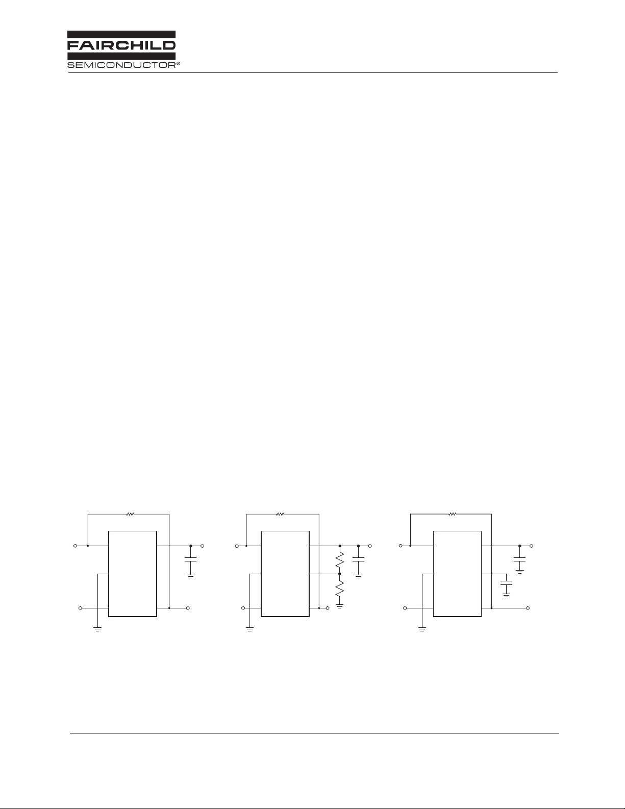
Typical Application
R
PG
FB
V
V
IN
OUT
SHDN
GND
CAP+
CAP-
EN
PG
FAN 2558
47KΩ47KΩ 47KΩ
R
PG
FB
V
V
IN
OUT
C
OUT
SHDN
GND
CAP+
CAP-
EN
FAN 2558ADJ
ADJ
PG
R
1
R
2
C
OUT
R
PG
FB
V
N
I
SHDN
GND
CAP+
CAP-
EN
FAN 2559
V
OUT
C
B
PG
C
OUT
YP
C
BYP
REV. 1.0.4 3/15/04

FAN2558/FAN2559 PRODUCT SPECIFICATIONS
Pin Assignments
TOP-VIEW
V
1
IN
2
GND
34
EN
V
5
V
OUT
PG
V
1
IN
2
GND
34
EN
6
V
5
ADJ/BYP
PG
OUT
NC/ADJ/BYP
OUT
PG
1
2
3
V
6
IN
5
GND
4
EN
FAN2558
5-Lead SOT-23 PACKAGE
FAN2558ADJ/FAN2559
6-Lead SOT-23 PACKAGE
FAN2558/FAN2558ADJ/FAN2559
2x2mm MLP-6 PACKAGE
Pin Name
Pin no.
FAN2558 FAN2558ADJ FAN2559
5SOT-23 2x2mm MLP-6 6SOT-23 2x2mm MLP-6 6SOT-23 2x2mm MLP-6
1V
IN
V
OUT
V
IN
V
OUT
V
IN
V
OUT
2 GND. NC GND. ADJ GND. BYP
3EN PG EN PGENPG
4PG EN PG ENPGEN
5V
OUT
6V
GND ADJ GND BYP GND
IN
V
OUT
V
IN
V
OUT
V
IN
Pin Descriptions
Symbol Pin Function Description
V
IN
V
OUT
GND Ground Connection
PG Power Good Output, Open Drain
ADJ Ratio of potential divider from V
BYP Reference Noise Bypass
EN Chip Enable Input. The regulator is fully enabled when TTL “H” is applied to this input. The regulator
Power Supply Input
Regulated Voltage Output
to ADJ determines output voltage
out
enters into shutdown mode when TTL “L” is applied to this input.
2
REV. 1.0.4 3/15/04

≥
PRODUCT SPECIFICATIONS FAN2558/FAN2559
Absolute Maximum Ratings
Parameter Min. Max. Units
V
to GND 6V
IN
Voltage on any other pin to GND -0.3 V
Junction Temperature (T
) -55 150 °C
J
Storage Temperature -65 150 °C
Lead Soldering Temperature, 10 seconds 300 °C
Power Dissipation (P
) Internally
D
Electrostatic Discharge (ESD) Protection (Note1) HBM 4 kV
CDM 1
+ 0.3 V
IN
Limited
W
Recommended Operating Conditions
Parameter Min. Typ. Max. Units
Supply Voltage Range, V
Supply Voltage Range, V
IN
IN
for V
for V
< 2.0V 2.7 5.5 V
OUT
2.0V V
OUT
OUT
+ V
DROPOUT
5.5 V
Load Current 180 mA
Enable Input Voltage V
EN
Power Good Output Voltage Range V
PG
0V
0V
IN
IN
V
V
Junction Temperature -40 125 °C
Thermal Resistance-Junction to Ambient SOT-23 (Note 2) 235
Thermal Resistance-Junction to Case, 2mm x 2mm
75
°C/W
6-lead MLP
Notes:
1. Using Mil Std. 883E, method 3015.7 (Human Body Model) and EIA/JESD22C101-A (Charge Device Model)
2. Junction to ambient thermal resistance, Θ
copper plains, number of via used, diameter of via used, available copper surface, and attached heat sink characteristics.
, is a strong function of PCB material, board thickness, thickness and number of
JC
REV. 1.0.4 3/15/04
3

FAN2558/FAN2559 PRODUCT SPECIFICATIONS
Electrical Characteristics
V
= V
IN
min (note 5) to 5.5V, V
IN
are at 25°C.
Symbol Parameter Conditions Min. Typ. Max. Units
V
EN
= V
, I
LOAD
= 100 µ A, T
IN
= -40°C to +85°C, unless otherwise noted. Typical values
A
Note:
3. Guaranteed ±1% output voltage accuracy parts are available on customer request.
4. Measured at constant junction temperature using low duty cycle pulse testing.
5. V
min = 2.7V or (V
IN
4
+ 1V), whichever is greater.
OUT
REV. 1.0.4 3/15/04

PRODUCT SPECIFICATIONS FAN2558/FAN2559
DC Electrical Characteristics (Continued)
VIN = VIN min (note 5) to 5.5V, V
values are at 25°C.
Symbol Parameter Conditions Min. Typ. Max. Units
PSRR Power Supply Rejection Ratio DC to 100kHz
e
Output Noise BW: 300Hz to 50kHz
N
EN
= VIN, I
= 100µA, TA = -40°C to +85°C, unless otherwise noted. Typical
LOAD
50 dB
C
=1µF
OUT
C
I
LOAD
= 10nF
BYPASS
= 0 to 150mA
V
≤ 1.8V
OUT
30 µV
C
=1µF
OUT
C
I
LOAD
= 10nF
BYPASS
= 0 to 150mA
RMS
REV. 1.0.4 3/15/04 5
 Loading...