Fairchild FAN2110 service manual
FAN2110 — TinyBuck™
3-24V Input, 10A, High-Efficiency, Integrated
Synchronous Buck Regulator
FAN2110 — TinyBuck™, 3-24V Input, 10A, High-Efficiency, Integrated Synchronous Buck Regulator
September 2011
Features
Wide Input Voltage Range: 3V-24V
Wide Output Voltage Range: 0.8V to 80% V
IN
10A Output Current
1% Reference Accuracy Over Temperature
Over 93% Peak Efficiency
Programmable Frequency Operation: 200KHz to
600KHz
Fully Synchronous Operation with Integrated
Schottky Diode on Low-Side MOSFET Boosts
Efficiency
Internal Bootstrap Diode
Power-Good Signal
Starts up on Pre-Bias Outputs
Accepts Ceramic Capacitors on Output
External Compensation for Flexible Design
Programmable Current Limit
Under-Voltage, Over-Voltage, and Thermal
Shutdown Protections
Internal Soft-Start
5x6mm, 25-Pin, 3-Pad MLP Package
Applications
Servers & Telecom
Graphics Cards & Displays
Computing Systems
Point-of-Load Regulation
Set-Top Boxes & Game Consoles
Description
The FAN2110 TinyBuck™ is a highly efficient, small
footprint, constant frequency, 10A integrated
synchronous Buck regulator.
The FAN2110 contains both synchronous MOSFETs
and a controller/driver with optimized interconnects in
one package, which enables designers to solve highcurrent requirements in a small area with minimal
external components. Integration helps to minimize
critical inductances making component layout simpler
and more efficient compared to discrete solutions.
The FAN2110 provides for external loop compensation,
programmable switching frequency, and current limit.
These features allow design flexibility and optimization.
High frequency operation allows for all ceramic
solutions.
The summing current mode modulator uses lossless
current sensing for current feedback and over-current
protection. Voltage feedforward helps operation over a
wide input voltage range.
Fairchild’s advanced BiCMOS power process, combined
with low-R
efficient MLP package, provide the ability to dissipate
high power in a small package.
Output over-voltage, under-voltage, and thermal
shutdown protections help protect the device from
damage during fault conditions. FAN2110 also prevents
pre-biased output discharge during startup in point-ofload applications.
internal MOSFETs and a thermally
DS(ON)
Related Application Notes
TinyCalc™ Calculator Design Tool
AN-8022 — TinyCalc™ Calculator User Guide
Ordering Information
Operating
Part Number
FAN2110MPX -10°C to 85°C Molded Leadless Package (MLP) 5x6mm Tape and Reel
FAN2110EMPX -40°C to 85°C Molded Leadless Package (MLP) 5x6mm Tape and Reel
© 2008 Fairchild Semiconductor Corporation www.fairchildsemi.com
FAN2110 • Rev. 1.0.3
Temperature Range Package
Packing
Method
Typical Application
FAN2110 — TinyBuck™, 3-24V Input, 10A, High-Efficiency, Integrated Synchronous Buck Regulator
IN
C
HF
Power
Enable
Good
P2
+5V
C
IN
C2
R2
C4
R
RAMP
R
ILIM
C1
R
T
VCC
RAMP
PGOOD
EN
ILIM
R(T)
COMP
AGND
15
25
13
14
17
18
20
16
Boot
Diode
PWM
+
DRIVER
Q1
Q2
POWER
MOSFETS
1
P1
P3
24
19
BOOT
SW
PGND
NC
FB
C
BOOT
OUT
L
C
OUT
R1
R
BIAS
C3
R3
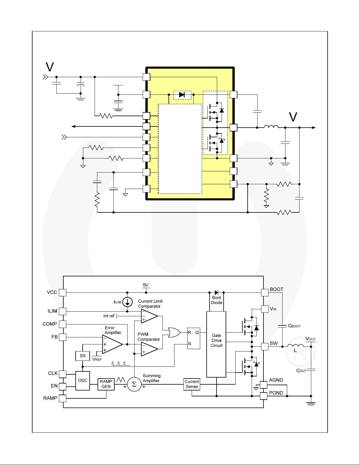
Figure 1. Typical Application Diagram
Block Diagram
Figure 2. Block Diagram
© 2008 Fairchild Semiconductor Corporation www.fairchildsemi.com
FAN2110 • Rev. 1.0.3 2
Pin Configuration
FAN2110 — TinyBuck™, 3-24V Input, 10A, High-Efficiency, Integrated Synchronous Buck Regulator
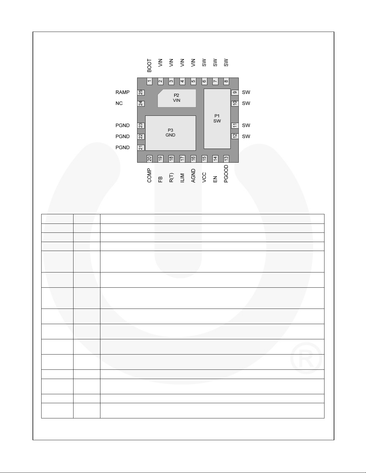
Figure 3. MLP 5x6mm Pin Configuration (Bottom View)
Pin Definitions
Pin # Name Description
P1, 6-12 SW
P2, 2-5 VIN
P3, 21-23 PGND
1 BOOT
13 PGOOD
14 EN
15 VCC
16 AGND
17 ILIM
18 R(T)
19 FB
20 COMP
24 NC
25 RAMP
Switching Node. Junction of high-side and low-side MOSFETs.
Power Conversion Input Voltage. Connect to the main input power source.
Power Ground. Power return and Q2 source.
High-Side Drive BOOT Voltage. Connect through capacitor (C
an internal synchronous bootstrap diode to recharge the capacitor on this pin to VCC when
SW is LOW.
Power-Good Flag. An open-drain output that pulls LOW when FB is outside the limits
specified in electrical specs. PGOOD does not assert HIGH until the fault latch is enabled.
ENABLE. Enables operation when pulled to logic HIGH or left open. Toggling EN resets the
regulator after a latched fault condition. This input has an internal pull-up when the IC is
functioning normally. When a latched fault occurs, EN is discharged by a current sink.
Input Bias Supply for IC. The IC’s logic and analog circuitry are powered from this pin. This
pin should be decoupled to AGND through a > 2.2µF X5R / X7R capacitor.
Analog Ground. The signal ground for the IC. All internal control voltages are referred to
this pin. Tie this pin to the ground island/plane through the lowest impedance connection.
Current Limit. A resistor (R
limit trip threshold lower than the internal default setting.
Oscillator Frequency. A resistor (R
frequency.
Output Voltage Feedback. Connect through a resistor divider to the output voltage.
Compensation. Error amplifier output. Connect the external compensation network between
this pin and FB.
No Connect. This pin is not used.
Ramp Amplitude. A resistor (R
and provides voltage feedforward functionality.
) to SW. The IC includes
BOOT
) from this pin to AGND can be used to program the current-
ILIM
) from this pin to AGND sets the PWM switching
T
) connected from this pin to VIN sets the ramp amplitude
RAMP
© 2008 Fairchild Semiconductor Corporation www.fairchildsemi.com
FAN2110 • Rev. 1.0.3 3
FAN2110 — TinyBuck™, 3-24V Input, 10A, High-Efficiency, Integrated Synchronous Buck Regulator
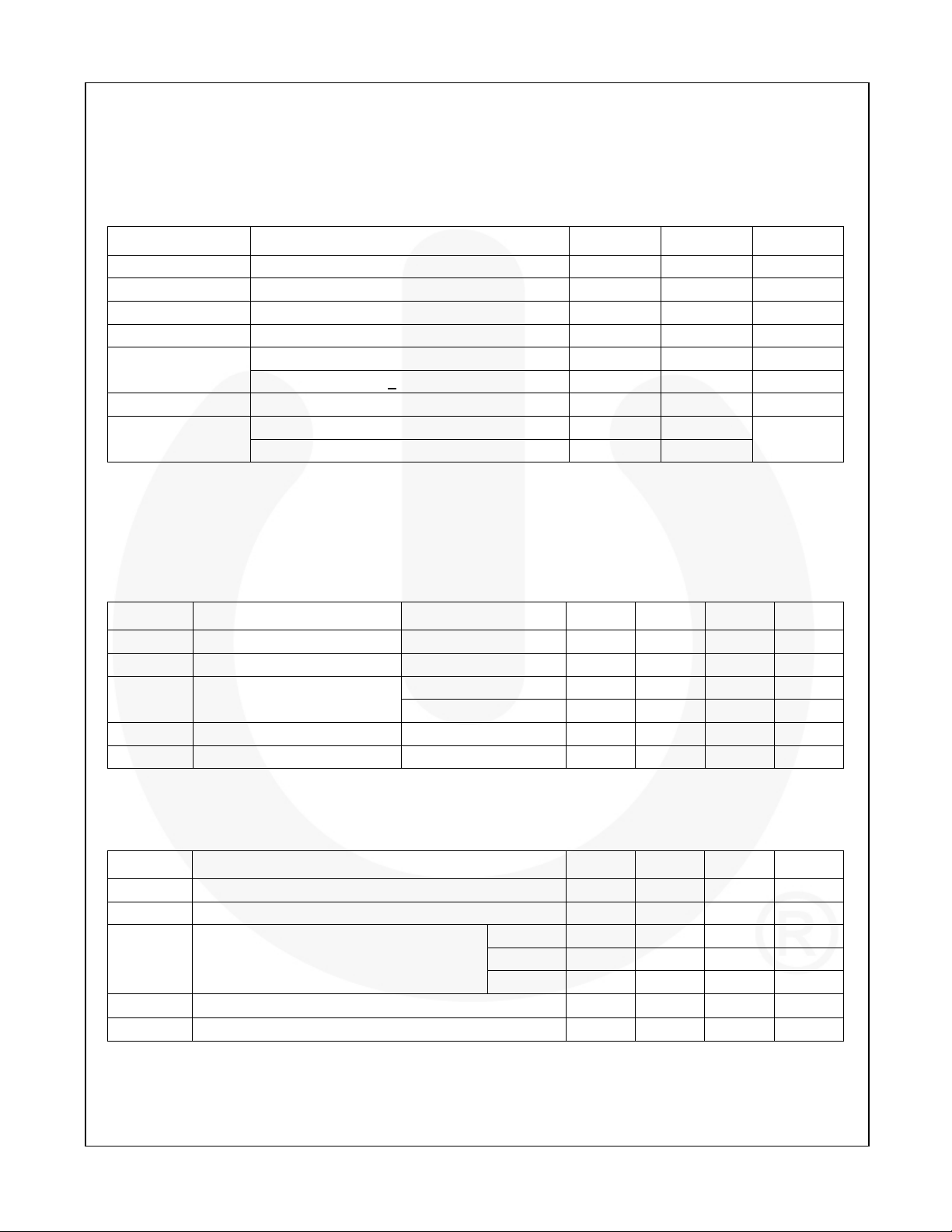
Absolute Maximum Ratings
Stresses exceeding the absolute maximum ratings may damage the device. The device may not function or be
operable above the recommended operating conditions and stressing the parts to these levels is not recommended.
In addition, extended exposure to stresses above the recommended operating conditions may affect device reliability.
The absolute maximum ratings are stress ratings only.
Parameter Conditions Min. Max. Unit
VIN to PGND 28 V
VCC to AGND AGND=PGND 6 V
BOOT to PGND 35 V
BOOT to SW -0.5 6.0 V
SW to PGND
All other pins -0.3 VCC+0.3 V
ESD
Continuous -0.5 24.0 V
Transient (t < 20ns, f < 600KHz) -5 30 V
Human Body Model, JEDEC JESD22-A114 2.0
Charged Device Model, JEDEC JESD22-C101 2.5
KV
Recommended Operating Conditions
The Recommended Operating Conditions table defines the conditions for actual device operation. Recommended
operating conditions are specified to ensure optimal performance to the datasheet specifications. Fairchild does not
recommend exceeding them or designing to absolute maximum ratings.
Symbol Parameter Conditions Min. Typ. Max. Unit
VCC Bias Voltage VCC to AGND 4.5 5.0 5.5 V
VIN Supply Voltage VIN to PGND 3 24 V
TA Ambient Temperature
TJ Junction Temperature +125 °C
fSW Switching Frequency 200 600 kHz
FAN2110MPX -10 +85 °C
FAN2110EMPX -40 +85 °C
Thermal Information
Symbol Parameter Min. Typ. Max. Unit
T
Storage Temperature -65 +150 °C
STG
TL Lead Soldering Temperature, 10 Seconds +300 °C
P1 (Q2) 4 °C/W
JC
J-PCB
PD Power Dissipation, TA=25°C
Note:
1. Typical thermal resistance when mounted on a four-layer, two-ounce PCB, as shown in Figure 35. Actual results
are dependent on mounting method and surface related to the design.
Thermal Resistance: Junction-to-Case
Thermal Resistance: Junction-to-Mounting Surface
(1)
2.8 W
P2 (Q1) 7 °C/W
P3 4 °C/W
(1)
35 °C/W
© 2008 Fairchild Semiconductor Corporation www.fairchildsemi.com
FAN2110 • Rev. 1.0.3 4
FAN2110 — TinyBuck™, 3-24V Input, 10A, High-Efficiency, Integrated Synchronous Buck Regulator
Electrical Specifications
Electrical specifications are the result of using the circuit shown in Figure 1 with VIN=12V, unless otherwise noted.
Symbol Parameter Conditions Min. Typ. Max. Unit
Power Supplies
SW=Open, V
f
=600KHz
ICC VCC Current
SW
Shutdown: EN=0, VCC=5V 7 10 µA
V
VCC UVLO Threshold
UVLO
Rising VCC 4.1 4.3 4.5 V
Hysteresis 300 mV
Oscillator
R
=50K to GND
fSW Frequency
T
RT=24K to GND
t
Minimum On-Time
ONmin
V
Ramp Amplitude, Peak-to-Peak
RAMP
t
Minimum Off-Time
OFFmin
(2)
50 65 ns
, 1.8V
16V
IN
=200K
R
(2)
100 150 ns
RAMP
Reference
VFB
Reference Voltage (see Figure 4 for
Temperature Coefficient)
FAN2110MPX, 25°C 794 800 806 mV
FAN2110EMPX, 25°C 795 800 805 mV
Error Amplifier
G DC Gain
GBW Gain Bandwidth Product
V
Output Voltage
COMP
I
Output Current, Sourcing VCC=5V, V
SINK
I
Output Current, Sinking VCC=5V, V
SOURCE
I
FB Bias Current VFB=0.8V, 25°C -850 -650 -450 nA
BIAS
(2)
(2)
12 15 MHz
(2)
0.4 3.2 V
=5V
V
CC
Protection and Shutdown
R
=182 K, 25°C, fSW=500KHz,
I
LIM
I
ILIM
T
T
V
V
UVSD
V
V
FLT_HYS
Current Limit (see Circuit
Description)
I
Over-Temperature Shutdown
TSD
Over-Temperature Hysteresis
HYS
Over-Voltage Threshold 2 Consecutive Clock Cycles
OVP
Current VCC=5V, 25°C -11 -10 -9 µA
LIM
(2)
(2)
(2)
+30 °C
Under-Voltage Shutdown 16 Consecutive Clock Cycles
Fault Discharge Threshold Measured at FB Pin 250 mV
FLT
Fault Discharge Hysteresis Measured at FB Pin (VFB ~500mV) 250 mV
ILIM
=1.5V, R
V
OUT
16 Consecutive Clock Cycles
Internal IC Temperature
Soft-Start
tSS V
tEN Fault Enable/SSOK (T1.0)
to Regulation (T0.8)
OUT
f
=500KHz
(2)
6.7 ms
SW
=0.7V, VCC=5V,
FB
8 12 mA
255 300 345 KHz
540 600 660 KHz
, RT=30K,
OUT
0.53 V
80 85 dB
=2.2V 1.5 2.2 mA
COMP
=1.2V 0.8 1.2 mA
COMP
RAMP
=243K
(3)
12 14 16 A
+155 °C
(3)
110 115 121 %V
(3)
68 73 78 %V
OUT
OUT
5.3 ms
Continued on the following page…
© 2008 Fairchild Semiconductor Corporation www.fairchildsemi.com
FAN2110 • Rev. 1.0.3 5
FAN2110 — TinyBuck™, 3-24V Input, 10A, High-Efficiency, Integrated Synchronous Buck Regulator
Electrical Specifications (Continued)
Electrical specifications are the result of using the circuit shown in Figure 1 with VIN=12V, unless otherwise noted.
Symbol Parameter Conditions Min. Typ. Max. Unit
Control Functions
VEN EN Threshold, Rising VCC=5V 1.35 2.00 V
V
V
V
Notes:
2. Specifications guaranteed by design and characterization; not production tested.
3. Delay times are not tested in production. Guaranteed by design.
EN Hysteresis VCC=5V 250 mV
EN_HYS
REN EN Pull-Up Resistance VCC=5V 800
I
EN Discharge Current Auto-Restart Mode, VCC=5V 1 µA
EN_DISC
R
FB OK Drive Resistance 800
FBok
PGTH_LO
PGOOD LOW Threshold
PGTH_UP
V
PGOOD Output Low I
PG_LO
I
PGOOD Leakage Current V
PG_LK
FB < V
Cycles
FB > V
Cycles
OUT
PGOOD
, 2 Consecutive Clock
REF
(3)
, 2 Consecutive Clock
REF
(3)
-14 -11 -8
+7 +10 +13.5
< 2mA 0.4 V
=5V 0.2 1.0 µA
%V
K
REF
© 2008 Fairchild Semiconductor Corporation www.fairchildsemi.com
FAN2110 • Rev. 1.0.3 6
 Loading...