Fairchild FAN2013B service manual

FAN2013B — 2A Low-Voltage, Current-Mode
Synchronous PWM Buck Regulator
FAN2013B — 2A Low-Voltage, Current-Mode Synchronous PWM Buck Regulator
December 2010
Features
95% Efficiency, Synchronous Operation
Adjustable Output Voltage from 0.8V to 2.5V
4.5V to 5.5V Input Voltage Range
Up to 2A Output Current
Fixed-Frequency 1.2 MHz PWM Operation
Soft-Start Function
Excellent Load Transient Response
Power-Good Flag
Over-Voltage, Under-Voltage Lockout, Short-
Circuit, and Thermal Shutdown Protections
3x3mm 6-Lead MLP Package
Applications
Hard Disk Drive
Set-Top Box
Point-of-Load Power
Notebook Computer
Communications Equipment
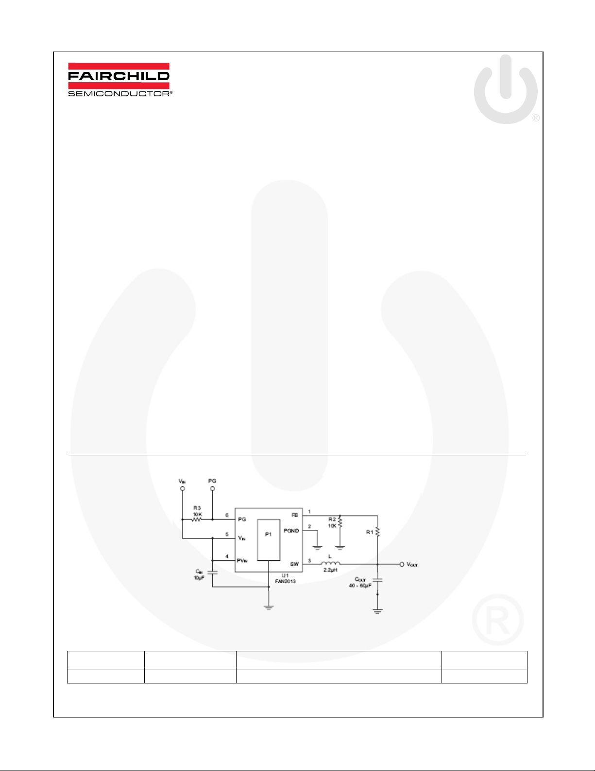
Typical Application
Description
The FAN2013B is a high-efficiency, low-noise,
synchronous Pulse Width Modulated (PWM) currentmode DC-DC converter designed for low-voltage
applications. It provides up to 2A continuous-load
current from the 4.5V to 5.5V input. The output voltage
is adjustable over a wide range by means of an external
voltage divider.
The FAN2013B is enabled when the input voltage on
the V
pin exceeds the UVLO threshold.
IN
A current-mode control loop with a fast transient
response ensures excellent line and load regulation.
The fixed 1.2MHz switching frequency enables
designers to choose a small, inexpensive external
inductor and capacitor. Filtering can be accomplished
with small components, reducing space and cost.
Protection features include input under-voltage lockout,
short-circuit protection, and thermal shutdown. Softstart limits inrush current during start-up conditions.
The device is available in a 3x3mm 6-lead MLP.
Figure 1. Typical Application
Ordering Information
Part Number Output Voltage Package Packing Method
FAN2013BMPX 0.8V to 2.5V 3x3mm 6-Lead Molded Leadless Package (MLP) Tape and Reel
© 2008 Fairchild Semiconductor Corporation www.fairchildsemi.com
FAN2013B • Rev. 1.0.2

Pin Assignments
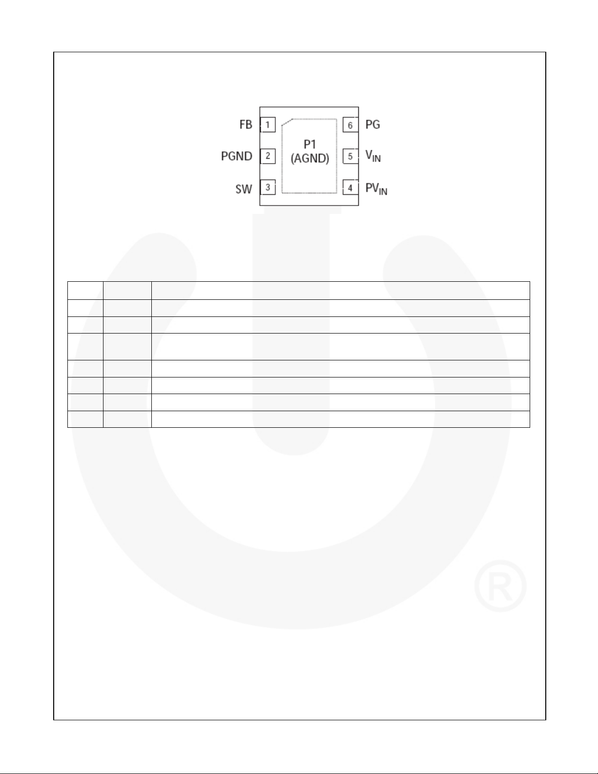
Figure 2. Pin Assignments (Top View)
Pin Definitions
Pin # Name Description
FAN2013B — 2A Low-Voltage, Current-Mode Synchronous PWM Buck Regulator
P1 AGND
1 FB
2 PGND
3 SW
4 PVIN
5 VIN
6 PG
Analog Ground. P1 must be soldered to the PCB ground.
Feedback Input. Adjustable voltage option; connect this pin to the resistor divider.
Power Ground. This pin is connected to the internal MOSFET switches. This pin must be
externally connected to AGND.
Switching Node. This pin is connected to the internal MOSFET switches.
Supply Voltage Input. This pin is connected to the internal MOSFET switches.
Supply Voltage Input.
Open Drain Power Good.
© 2008 Fairchild Semiconductor Corporation www.fairchildsemi.com
FAN2013B • Rev. 1.0.2 2

FAN2013B — 2A Low-Voltage, Current-Mode Synchronous PWM Buck Regulator
Absolute Maximum Ratings
Stresses exceeding the absolute maximum ratings may damage the device. The device may not function or be
operable above the recommended operating conditions and stressing the parts to these levels is not recommended.
In addition, extended exposure to stresses above the recommended operating conditions may affect device
reliability. The absolute maximum ratings are stress ratings only.
Symbol Parameter Min. Max. Unit
VIN Supply Voltage -0.3 7.0 V
Input Voltage on PVIN and Any Other Pin -0.3 VIN V
θJC
Thermal Resistance, Junction-to-Tab
TL Lead Soldering Temperature (10 Seconds) +260 °C
T
Storage Temperature -65 +150 °C
STG
TJ Junction Temperature -40 +150 °C
ESD
Electrostatic Discharge Protection
(2)
Level
Notes:
1. Junction-to-ambient thermal resistance, θJA, is a strong function of PCB material, board thickness, thickness and
number of copper planes, number of via used, diameter of via used, available copper surface, and attached heat
sink characteristics.
2. Using Mil Std. 883E, method 3015.7 (Human Body Model) and EIA/JESD22C101-A (Charged Device Model).
(1)
8 °C/W
Human Body Model,
JESD22-A114
Charged Device Model,
JESD22-C101
3.5
kV
2.0
Recommended Operating Conditions
The Recommended Operating Conditions table defines the conditions for actual device operation. Recommended
operating conditions are specified to ensure optimal performance to the datasheet specifications. Fairchild does not
recommend exceeding them or designing to Absolute Maximum Ratings.
Symbols Parameter Min. Typ. Max. Unit
VIN Supply Voltage Range 4.5 5.5 V
V
Output Voltage Range, Adjustable Version 0.8 2.5 V
OUT
I
Output Current 2.0 A
OUT
L Inductor
CIN Input Capacitor
C
Output Capacitor
OUT
TA Operating Ambient Temperature Range -40 +85 °C
Note:
3. Refer to the Applications section for details.
(3)
2.2 µH
(3)
10 20 µF
(3)
20 40 µF
© 2008 Fairchild Semiconductor Corporation www.fairchildsemi.com
FAN2013B • Rev. 1.0.2 3
 Loading...