Fairchild FAN1577A service manual

FAN1577A
Dual Synchronous DC/DC Controller
FAN1577A — Dual Synchronous DC/DC Controller
October 2010
Features
Integrates Two Sets of MOSFET Drivers
Two Independent PWM Controllers
Constant Frequency Operation: Free-running Fixed-
Frequency Oscillator Programmable: 61kHz to 340kHz
Maximum Input Supply Voltage: 15V
Programmable Output as Low as 0.7V
Internal Error Amplifier Reference Voltage:
0.7V ±1.0%
Two Soft-Start / EN Function Pins
Programmable Over-Current Protection (OCP)
30V HIGH Voltage Pin for Bootstrap Voltage
Output Over-Voltage Protection (OVP)
20-Pin SOP
Applications
CPU and GPU Vcore Power Supply
Power Supply Requiring Two Independent Outputs
Description
The FAN1577A is a high-efficiency, voltage-mode, dualchannel, synchronous DC/DC PWM controller for two
independent outputs. The two channels are operated
out of phase. The internal reference voltage is trimmed
to 0.7V±1.0%. It is connected to the error amplifier’s
positive terminal for voltage feedback regulation.
A soft-start circuit ensures the output voltage can be
gradually and smoothly increased from zero to its final
regulated value. The soft-start pin can also be used for
chip-enable function. When two soft-start pins are
grounded, the chip is disabled, and the total operation
current can be reduced to under 0.7mA.
The fixed-frequency is programmable from 61kHz to
340kHz. The Over-Current Protection (OCP) level can
be programmed by an external current-sense resistor. It
has two integrated sets of internal MOSFET drivers.
FAN1577A is available in a 20-pin small-outline
package (SOP).
Ordering Information
Part Number Operating Temperature Range Package Packing Method
FAN1577AMX -40°C to +85°C 20-Lead, Small-Outline Package Tape & Reel
© 2010 Fairchild Semiconductor Corporation www.fairchildsemi.com
FAN1577A • Rev. 1.0.0

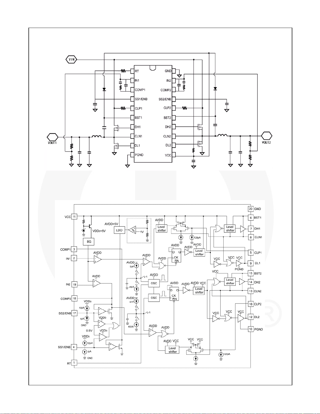
Application Diagram
FAN1577A — Dual Synchronous DC/DC Controller
Figure 1. Typical Application
Internal Block Diagram
Figure 2. Functional Block Diagram
© 2010 Fairchild Semiconductor Corporation www.fairchildsemi.com
FAN1577A • Rev. 1.0.0 2

AA
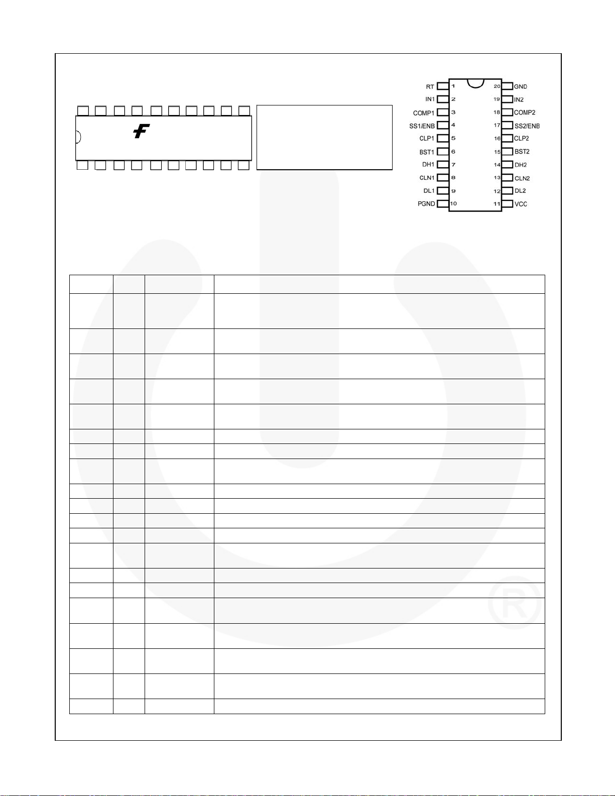
Pin Configuration & Marking Information
20
F: Fairchild Logo
TAHAA
FAN1577AM
T: Assembly Plant Code
A: Year Code
H: Week Code
: Die Run Code
1
Figure 3. Marking Diagram Figure 4. Marking Legend Figure 5. Pin Assignments
(Top View)
Pin Definitions
Name Pin # Type Description
RT 1
IN1 2 Feedback
COMP1 3 Compensation
SS1/ENB 4
CLP1 5
BST1 6 Boost Supply Supply for high-side driver. Connect to the internal bootstrap circuit.
DH1 7 High-Side Drive Channel 1, high-side MOSFET gate driver pin.
CLN1 8 Switch Node
DL1 9 Low-Side Drive Low-side MOSFET gate driver pin.
PGND 10 Driver Ground Driver circuit reference. Connect to low-side MOSFET GND.
VCC 11 Power Supply Supply voltage input.
DL2 12 Low-Side Drive Low-side MOSFET gate driver pin.
CLN2 13 Switch Node
DH2 14 High-Side Drive Channel 2 high-side MOSFET gate driver pin.
BST2 15 Boost Supply Supply for high-side driver. Connect to the internal bootstrap circuit.
CLP2 16
SS2/ENB 17
COMP2 18 Compensation
IN2 19 Feedback
GND 20 Analog Ground The reference of internal control circuits.
Frequency
Select
Soft-Start /
Enable
Over-Current
Protection
Over-Current
Protection
Soft-Start /
Enable
An external resistor connecting this pin to GND can program the switching
frequency. The switching frequency is 61kHz when RT is open and becomes
340kHz when RT is shorted to ground.
Inverting input of the error amplifier normally connected to the switching power
supply output through a resistor divider.
Output of the error amplifier and input to the PWM comparator. It is used for
feedback-loop compensation.
A 35/15µA internal current source charging an external capacitor for soft-start.
Pull down this pin and pin 17 to disable the chip.
Over-current protection for high-side MOSFET. Connect a resistor from this pin
to the high-side supply voltage to program the OCP level.
Switch-node connection to the inductor. For channel 1, high-side driver’s
reference ground.
Switch-node connection to the inductor. For channel 2, high-side driver’s
reference ground.
Over-current protection for the high-side MOSFET. Connect a resistor from this
pin to the high-side supply voltage to program the OCP level.
A 35/15µA internal current source charging an external capacitor for soft-start.
Pull down this pin and pin 4 to disable the chip.
Output of the error amplifier and input to the PWM comparator. It is used for
feedback-loop compensation.
Inverting input of the error amplifier. It is normally connected to the switching
power supply output through a resistor divider.
FAN1577A — Dual Synchronous DC/DC Controller
© 2010 Fairchild Semiconductor Corporation www.fairchildsemi.com
FAN1577A • Rev. 1.0.0 3

FAN1577A — Dual Synchronous DC/DC Controller
Absolute Maximum Ratings
Stresses exceeding the absolute maximum ratings may damage the device. The device may not function or be
operable above the recommended operating conditions and stressing the parts to these levels is not recommended.
In addition, extended exposure to stresses above the recommended operating conditions may affect device
reliability. The absolute maximum ratings are stress ratings only. All voltage values, except differential voltages, are
given with respect to the network ground terminal.
may cause permanent damage to the device.
Symbol Parameter Min. Max. Unit
VCC Supply Voltage, VCC to GND 16 V
BST1(or 2) –
CLN1(or 2)
CLN1(or 2) –
GND
BST1(or 2) –
GND
DH1(or 2) –
CLN1(or 2)
CLN1(or 2),
DL1(or 2)
PGND PGND to GND ±1 V
ΘJA Thermal Resistance, Junction-Air 70 °C/W
TJ Operating Junction Temperature -40 +125 °C
T
STG
ESD
BST1(2) to CLN1(2) 16 V
CLN1(2) to GND for 100ns Transient -4 18 V
BST1(2) to GND for 100ns Transient 30 V
16 V
-0.3 VCC+0.3 V
Storage Temperature Range -65 +150 °C
Electrostatic Discharge
Protection Level
Stresses beyond those listed under Absolute Maximum Ratings
Human Body Model (HBM) 2
Charged Device Model (CDM) 1
kV
Recommended Operating Conditions
The Recommended Operating Conditions table defines the conditions for actual device operation. Recommended
operating conditions are specified to ensure optimal performance to the datasheet specifications. Fairchild does not
recommend exceeding them or designing to absolute maximum ratings.
Symbol Parameter Min. Max. Unit
V
Supply Voltage +15 V
CC
TA Operating Ambient Temperature
-40
+85
°C
© 2010 Fairchild Semiconductor Corporation www.fairchildsemi.com
FAN1577A • Rev. 1.0.0 4

Electrical Characteristics
VCC=12V and TA= -40°C to +85°C unless otherwise noted.
Symbol Parameter Conditions Min. Typ. Max. Unit
VCC UVLO
V
Turn-On Threshold VCC Ramp-Up 9.5 10.0 10.5 V
CC_ON
V
UVLO Hysteresis VCC Ramp-Down 1.5 2.0 2.5 V
CC_HYS
Oscillator
=OPEN 55 61 67
R
F
Oscillator Frequency
OSC
F
Total Accuracy
OSC,RT
D
Maximum Duty Cycle 85 90 95 %
ON_MAX
RT
RRT=GND 308 340 372
20kΩ<R
RT
-10 10 %
Error Amplifier
V
Internal Reference Voltage VCC=8V, VCC=15V, TA=25°C 0.693 0.700 0.707 V
REF
△V
V
REF
A
Open-Loop Voltage Gain 77 DB
VOL
Temperature Coefficient
REF
(1)
TA=-40~85oC 0.03 MV/OC
BW Unity Gain Bandwidth 3.5 MHZ
I
Output Source Current IN1=IN2=0.6V 60 80 100 µA
SOURCE
I
Output Sink Current IN1=IN2=0.8V 250 400 600 µA
SINK
V
H RAMP_PEAK
V
RAMP_VALLEY
Peak of VRAMP Gate Output=D
2.45 2.80 3.15 V
ON_MAX
Valley of VRAMP No Gate Output 1.05 1.20 1.35 V
Two-Stage Soft-Start
I
SRC_1
I
SRC_2
V
SS_TRANSITION
1st Soft-Start Charge Current
2nd Soft-Start Charge Current
Soft-Start Transition Point
V
CLP<VCLN
V
CLP<VCLN
I
SOURCE_1
I
SOURCE_2
, V
SS_Transition>VSS
, V
SS_Transition<VSS
st
Transit to
nd
28 35 42 µA
13 16 19 µA
1.40 1.42 1.44 V
See Figure 6
I
Soft-Start Discharge Current
SINK
V
CLP>VCLN
50 µA
Protections
I
OC Sink Current VCC=12V 90 120 150 µA
OCSET
TOT Over-Temperature 150 °C
T
Over-Temperature Hysteresis 20 °C
OT_HYS
V
Over-Voltage Protection of IN V
OVP
118 122 126 %
OVP/VIN
Output
IDH High-Side Current Source
RDH High-Side Sink Resistor V
I
DL
Low-Side Current Source VCC=12V, V
BST
V
CLN
BST
=12V, V
CLN
=6V
- V
=12V 2.8 3.8 Ω
CLN
=6V 1.0 1.8 A
DL
DH
-
1.0 1.8 A
V
- V
RDL Low-Side Sink Resistor VCC=12V 2.8 3.8 Ω
TDT Dead Time
(2)
V
=12V, DH & DL=1000pF 50 70 90 NS
CC
Total Operating Current
I
Operating Supply Current VCC=12V, No Load 3.3 4.3 5.3 MA
CC_OP
I
Standby Current (Disabled) SS1/ENB=SS2/ENB=0V 0.7 1.0 MA
CC_SBY
Notes:
1. Not tested in production; 30 pieces sampled.
2. When V
© 2010 Fairchild Semiconductor Corporation www.fairchildsemi.com
FAN1577A • Rev. 1.0.0 5
falls less than 2V relative to VDH rising to 2V.
DL
KHZ
FAN1577A — Dual Synchronous DC/DC Controller
 Loading...