Fairchild ES1A, ES1D service manual

Features
• For surface mount applications.
• Glass passivated junction.
• Low profile package.
• Easy pick and place.
• Built-in strain relief.
• Superfast recovery times for
high efficiency.
Fast Rectifiers
ES1A - ES1D
ES1A - ES1D
SMA/DO-214AC
COLOR BAND DENOTES CATHODE
Absolute Maximum Ratings* T
Symbol
V
Maximum Repetitive Reverse Voltage 50 100 150 200 V
RRM
I
Average Rectified Forward Current, @ TA=120°C 1.0 A
F(AV)
I
Non-repetitive Peak Forward Surge Current
FSM
T
stg
TJ Operating Junction Temperature -50 to +150
8.3 ms Single Half-Sine-Wave
Storage Temperature Range -50 to +150
Parameter
= 25°C unless otherwise noted
A
1A 1B 1C 1D
Value
Units
30 A
C
°
C
°
*These ratings are limiting values above which the serviceability of any semiconductor device may be impaired.
Thermal Characteristics
Symbol
PD Power Dissipation 1.47 W
R
θJA
R
θJL
Thermal Resistance, Junction to Ambient* 85
Thermal Resistance, Junction to Lead* 35
*Device mounted on FR-4 PCB 0.013 mm.
Electrical Characteristics T
Symbol
VF Forward Voltage @ 1.0 A 0.92 V
trr Reverse Recovery Time
I
= 0.5 A, IR = 1.0 A, I
IR
CT Total Capacitance
F
Reverse Current @ rated V
VR = 4.0 V, f = 1.0 MHz
Parameter
Parameter
= 0.25 A
RR
R TA
T
= 25°C unless otherwise noted
A
= 25°C
= 100°C
A
Value
Device
1A 1B 1C 1D
15 ns
5.0
100
7.0 pF
Units
C/W
°
C/W
°
Units
A
µ
A
µ
ES1A-ES1D, Rev. C12010 Fairchild Semiconductor Corporation

Typical Characteristics
ES1A - ES1D
1.5
[A]
F
1.25
1
0.75
RESISTIVE O R
INDUCTIVE LOAD
P.C . B. M O UN T E D
0.5
ON 0.2 x 0.2"
(5. 0 x 5.0 mm)
COPPER PAD AREAS
0.25
0
0 25 50 75 100 125 150 175
Average Rectified Forward Current, I
Ambient Temperature [ºC]
10
1
[A]
F
0.1
0.01
Forward Current, I
0.001
0.4 0.6 0.8 1 1.2 1.4
T = 25 C
º
A
Pulse Width = 300
2% Duty Cycle
µµµµ
Forward Voltage, VF [V]
s
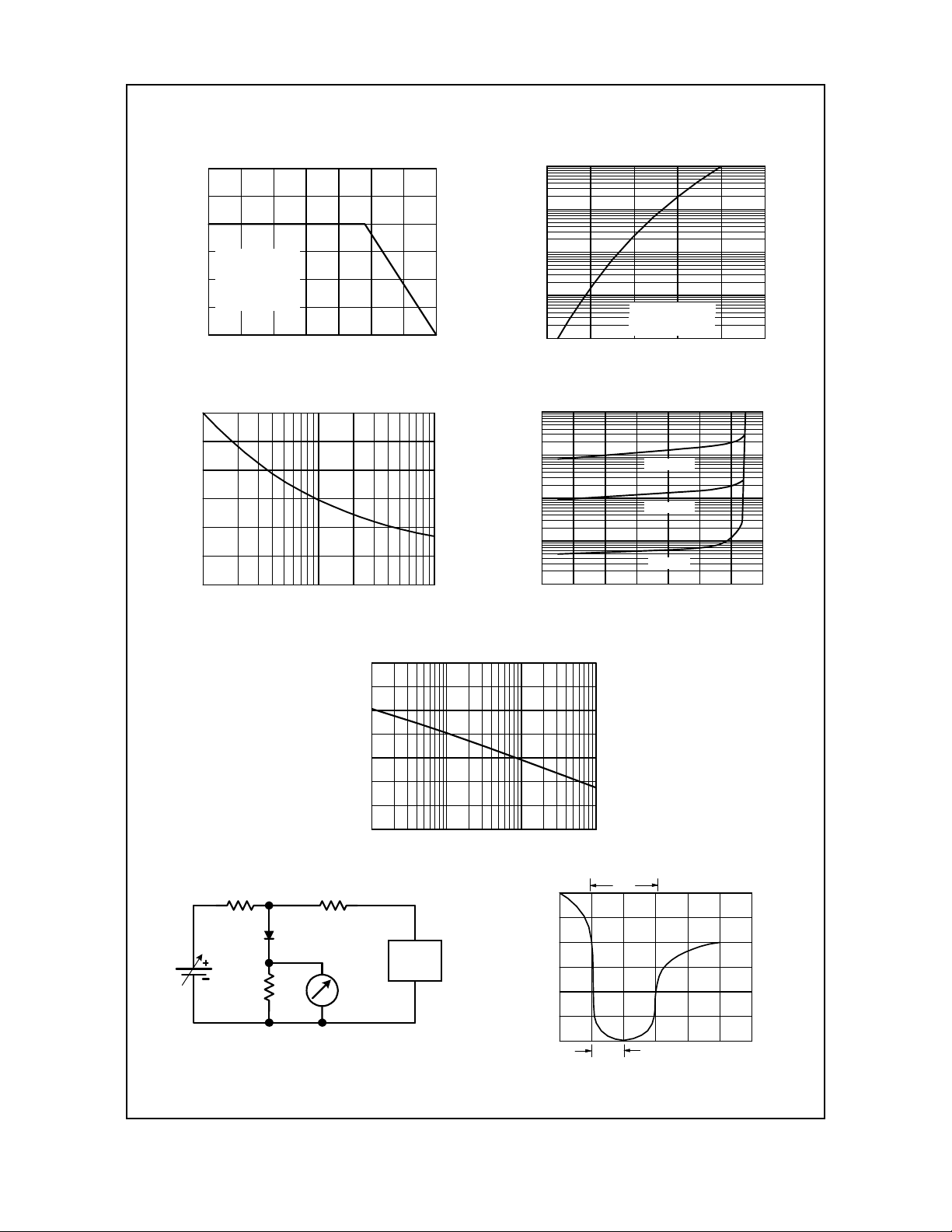
Figure 1. Forward Current Derating Curve Figure 2. Forward Voltage Characteristics
30
[A]
25
FSM
20
15
10
5
0
12 51020 50100
Peak Forward Surge Current, I
Number of Cycles at 60Hz
1000
[uA]
R
100
10
T = 125 C
º
A
T = 75 C
º
A
1
T = 25 C
Reverse Current, I
0.1
0 20406080100120140
º
A
Percent of Rated Peak Reverse Voltage [%]
Figure 3. Non-Repetitive Surge Current Figure 4. Reverse Current vs Reverse Voltage
14
12
[pF]
T
10
8
6
4
2
Total Capacitance, C
0
0.1 1 10 100
Figure 5. Total Capacitance
50
Ω
NONINDUCTIVE
50V
(approx)
50Ω
NONINDUCTIVE
NOTES:
1. Rise time = 7.0 ns max; Input impedance = 1.0 megaohm 22 pf.
2. Rise time = 10 ns max; Source impedance = 50 ohms.
50Ω
NONINDUCTIVE
DUT
OSCILLOSCOPE
(Note 1)
(-)
Pulse
Generator
(Note 2)
(+)
Reverse Recovery Time Characterstic and Test Circuit Diagram
Reverse Voltage, VR [V]
+0.5A
-0.25A
-1.0A
trr
0
1.0cm SET TIME BASE FOR
5/ 10 ns/ cm
ES1A-ES1D, Rev. C12010 Fairchild Semiconductor Corporation
 Loading...