FSAV331
Dual Channel 4:1 Video Switch
FSAV331 Dual Channel 4:1 Video Switch
April 2004
Revised August 2005
General Description
The Fairchild video switch FSAV331 is a dual 4:1 high speed
video switch which can be configured as either multiplexer or
demultiplexer. Low On Resistance allows inputs to be connected to outputs without adding propagation delay or generating additional ground bounce noise.
When the OE Pin is LOW, S
selected B Port output. When the OE Pin is HIGH, the switch is
OPEN and a HIGH-Impedance state exists between the two
ports.
and S1 connect the A Port to th e
0
Features
O
Wide bandwidth: 300 MHz
O
73 dB non adjacent channel crosstalk at 10MHz
O
56 dB Off Isolation at 10MHz
O3:
typical On Resistance (RON)
O
Low power consumption (3uA maximum)
O
Control input: TTL compatible
Applications
O
Y/C video or CVBS video switch in LCD, plasma,
and projector displays
Ordering Code:
Order Number Package Number Package Description
FSAV331QSC MQA16A 16-Lead Quarter Size Small Outline Package (QSOP), JEDEC MO-137, 0.150" Wide
FSAV331MTC MTC16 16-Lead Thin Shrink Small Outline Package (TSSOP), JEDEC MO-153, 4.4mm Wide
Device also available in Tape and Reel. Specify by appending suffix letter “X” to the ordering code.
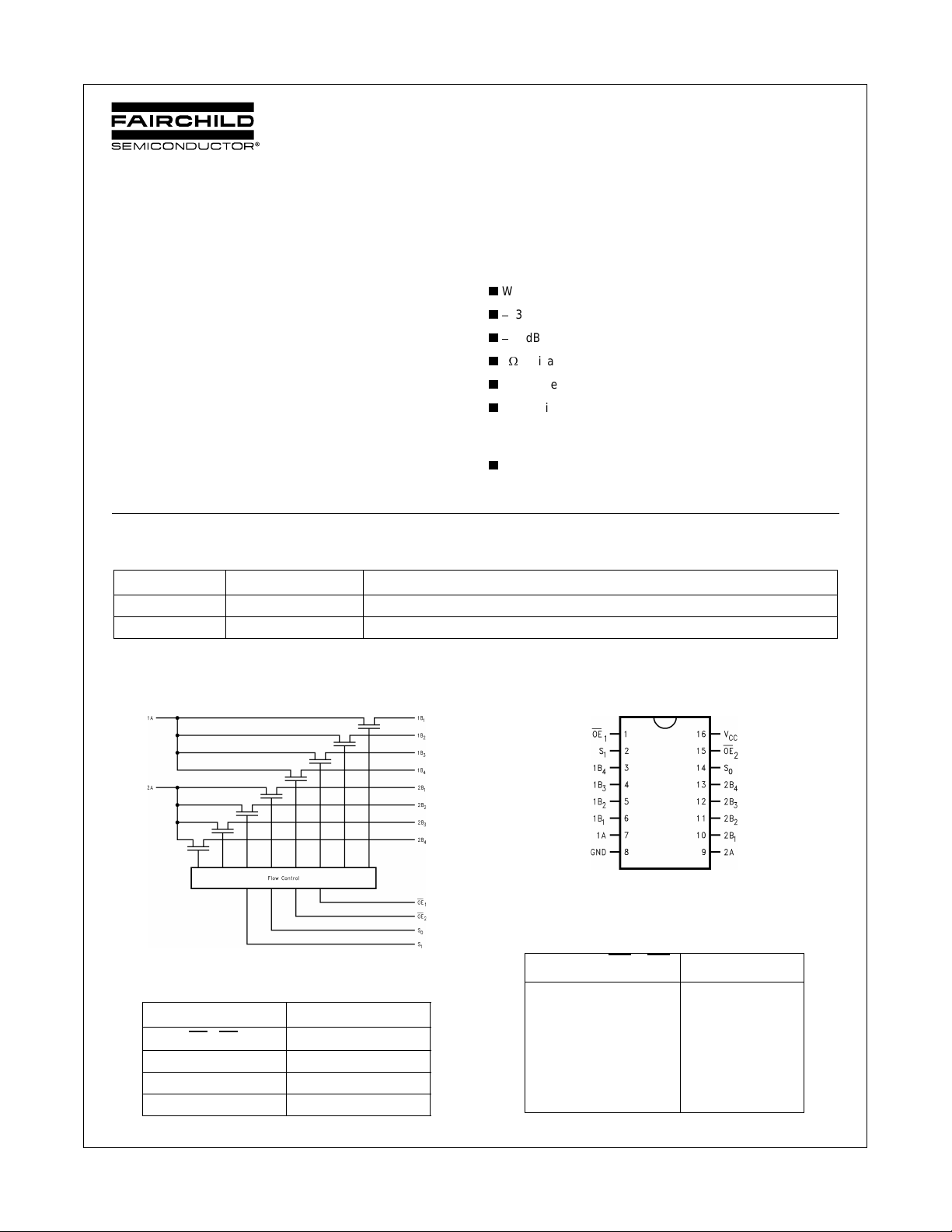
Logic Diagram
Connection Diagram
Truth Table
Pin Descriptions
Pin Name Description
OE1, OE
B
1
© 2005 Fairchild Semiconductor Corporation DS500802 www.fairchildsemi.com
2
S
, S
0
1
ABus A
, B2, B3, B
4
Bus Switch Enables
Select Inputs
Bus B
S1S0OE1OE
X X H X Disconnect 1A
X X X H Disconnect 2A
LLLL A = B
LHLL A = B
HLLL A = B
HH L L A = B
2
Function
1
2
3
4

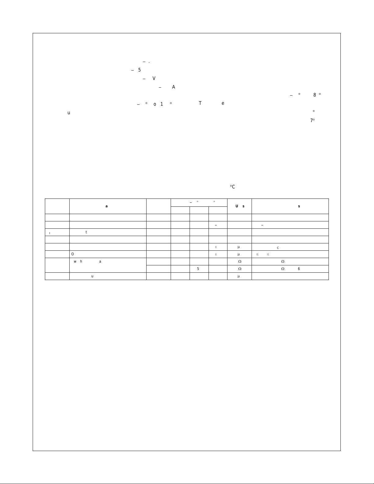
Absolute Maximum Ratings(Note 1)
FSAV331
Supply Voltage (VCC)
DC Switch Voltage (Note 2)
DC Input Voltage (V
) (Note 2)
IN
DC Input Diode Current
DC Output Current 128 mA
Storage Te mperature Range (T
STG
ESD (Human Body Model) 2000V
0.5V to +7.0V
0.5V to VCC + 0.5V
0.5V to +7.0V
50 mA
)65qC to +150 qC
Recommended Operating Conditions
(Note 3)
Supply Voltage (V
Control Input Voltage 0V to V
Switch Input Voltage 0V to V
Operating Temperature
Thermal Resistance
(TSSOP) 100
(QSOP) 127
Note 1: The Absolute Maximum Ratings are those values beyond which the safety of
the device cannot be guaranteed. The device should not be operated at these limits.
The parametric values defined in the Electrical Characteristics tables are not guaranteed at the absolute maximum rating. The Recommended Operating Conditions
tables will define the conditions for actual device operation.
Note 2: The input and output negative voltage ratings may be exceeded if the input
and output diode current ratings are observed.
Note 3: Unused control inputs must be held HIGH or LOW. They may not float.
) 4.75V to 5.25V
CC
40q
C to +85qC
q
C/W
q
C/W
CC
CC
DC Electrical Characteristics All typical value are for V
V
Symbol Parameter
V
ANALOG
V
IK
V
IH
V
IL
I
IN
I
OZ
R
ON
I
CC
Note 4: Measured by the voltage drop between A and B Pins at the indicated current through the switch. On Resistance is determined by the lower of the voltages on the two
(A or B Ports).
Analog Signal Range 4.75 - 5.25 0 2.0 V
Clamp Diode Voltage 4.75
Input Voltage HIGH 4.75 - 5.25 2.0 V
Input Voltage LOW 4.75 - 5.25 0.8 V
Control Input Leakage 5.25
OFF-STATE Leakage Current 5.25
Switch On Resistance 4.75 3.3 7.0
(Note 4) 4.75 5.0 10.0
Quiescent Supply Current 5.25 3.0
CC
(V) Min Typ Max
TA = 40 qC to +85 qC
= 5V @ 25qC unless otherwise specified.
CC
Units Conditions
1.2 V IIN = 18 mA
r
1.0
r
1.0
P
AVIN = 0V to V
P
A0 d A, B d V
:
VIN = 1V, RL = 75:, ION = 13 mA
:
VIN = 2V, RL = 75:, ION = 26 mA
P
AVIN = 0V or VCC, I
CC
CC
OUT
= 0V
www.fairchildsemi.com 2

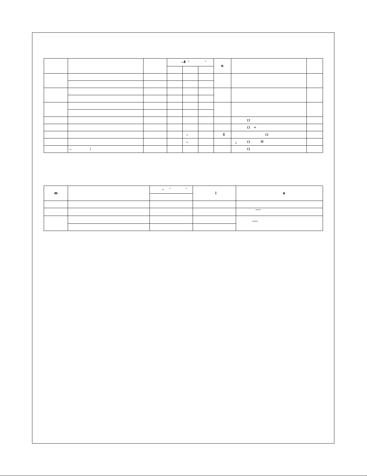
AC Electrical Characteristics
FSAV331
Symbol Parameter
t
ON
t
OFF
t
PLH
t
PHL
DG Differential Gain 4.75 to 5.25 0.26 % RL = 150:, f = 3.58MHz
DP Differential Phase 4.75 to 5.25 0.23 Degree RL = 150:, f = 3.58MHz
O
IRR
X
TALK
BW
Note 5: This specification is guaranteed by design.
Turn ON Time S-to-Bus B 4.75 to 5.25 1.0 5.3
Output Enable Time OE-to-A or B 4.75 to 5.25 1.0 5.3
Turn OFF Time S-to-Bus B 4.75 to 5.25 1.0 5.8
Output Disable Time OE-to-A or B 4.75 to 5.25 1.0 5.5
, Propagation Delay (Note 5) 4.75 to 5.25 0.1
Select-to-Bus A Delay 4.75 to 5.25 5.0
Non Adjacent OFF-Isolation 4.75 to 5.25
Non Adjacent Channel Crosstalk 4.75 to 5.25
3dB Bandwidth 4.75 to 5.25 300 MHz RL = 150
V
(V) Min Typ Max Number
CC
TA = 40 qC to +85 qC
56.0 dB f = 10MHz, RL = 150
73.0 dB RL = 150:, f = 10MHz Figure 4
Units Conditions
ns VI = 7V for t
ns VI = 7V for t
ns VI OPEN
and VI = OPEN for t
PZL
and VI = OPEN for t
PLZ
:
Capacitance
= 40 qC to +85 qC
T
Symbol Parameter
C
IN
C
ON
C
OFF
Control Pin Input Capacitance 3.0 pF VCC = 5.0V
A/B On Ca pacitance 39.0 pF VCC = 5.0, OE = 0V
Port B OFF Capacitance 5.0 pF
Port A OFF Capacitan ce 13.0 pF
A
Typ
Units Conditions
VCC and OE = 5.0V
Figure
PZH
PHZ
:
Figures
1, 2
Figures
1, 2
Figures
1, 2
Figure 3
Figure 5
3 www.fairchildsemi.com
 Loading...