Fairchild DM7442A service manual

查询7442供应商
DM7442A
BCD to Decimal Decoder
DM7442A BCD to Decimal Decoder
August 1986
Revised February 2000
General Description
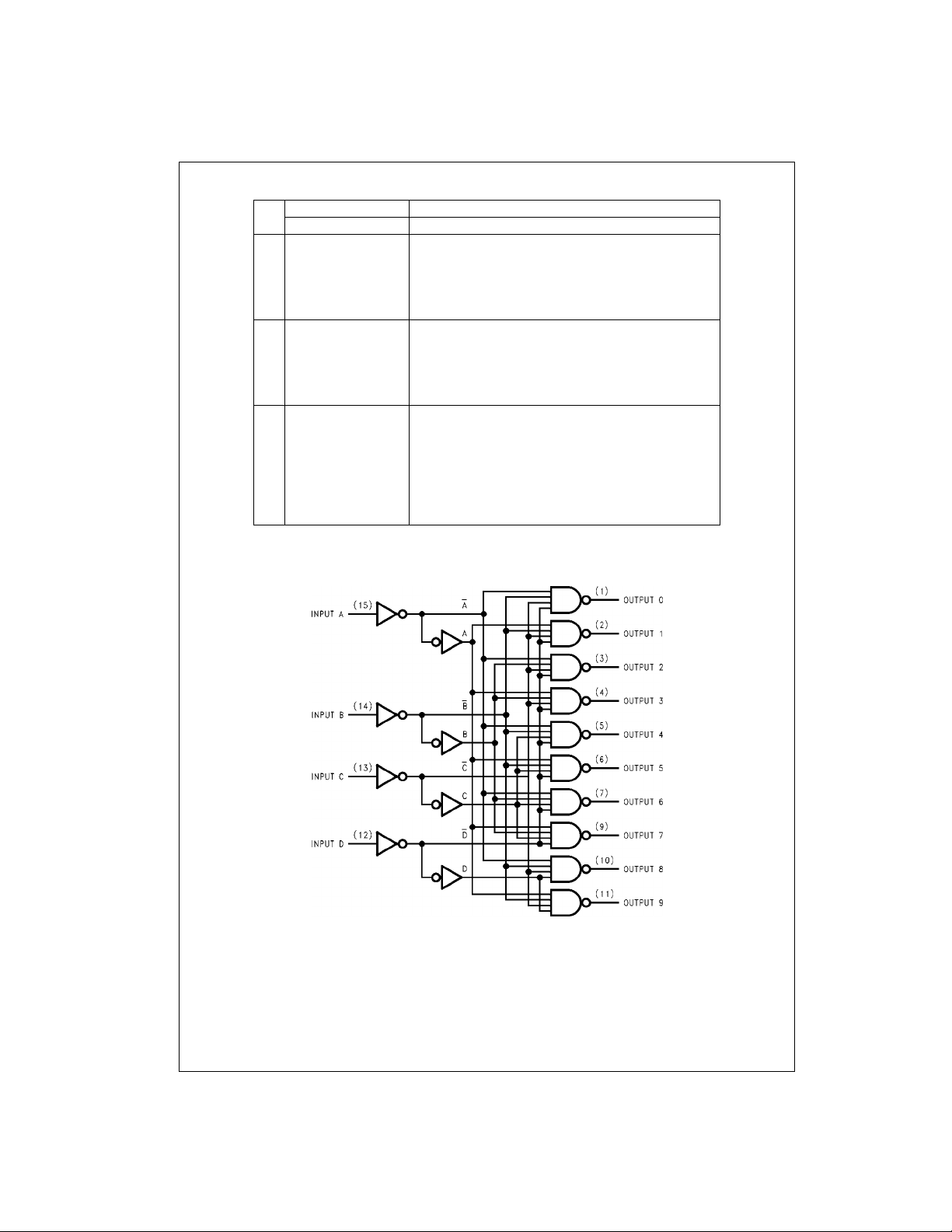
These BCD-to-decimal de coders consist of eig ht inverters
and ten, four-input NAND gates. The inverters are connected in pairs to make BCD input data available for
decoding by the NAND gat es. Full decoding of input logic
ensures that all outputs remai n off for all invalid (10–15)
input conditions.
Features
■ Diode clamped inputs
■ Also for application as 4-line-to-16-line decoders;
3-line-to-8-line decoders
■ All outputs are high for invalid input conditions
■ Typical power d issipation 140 mW
■ Typical propagation delay 17 ns
Ordering Code:
Order Number Package Number Package Description
DM7442AN N16E 16-Lead Plastic Dual-In-Line Package (PDIP), JEDEC MS-001, 0.300 Wide
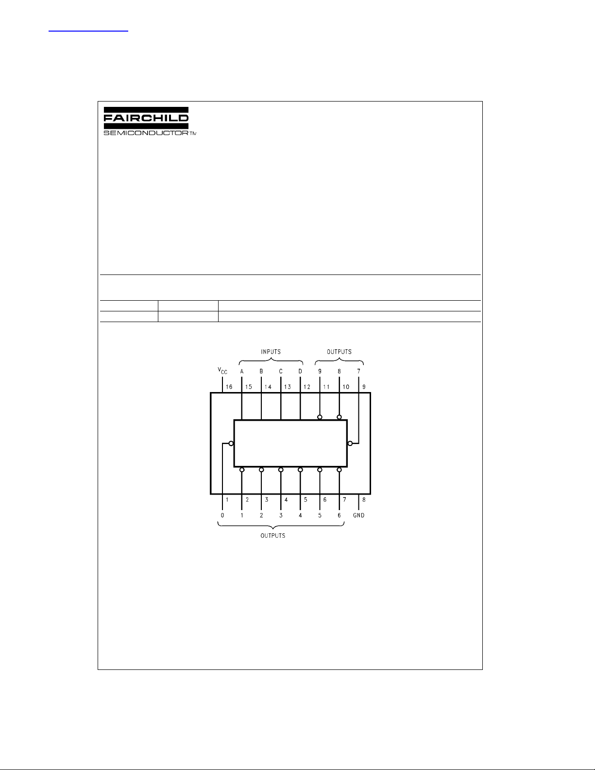
Connection Diagram
© 2000 Fairchild Semiconductor Corporation DS006516 www.fairchildsemi.com

Function Table
DM7442A
H = HIGH Level
L = LOW Level
Logic Diagram
No. BCD Input Decimal Output
DCBA0123456789
0LLLLLHHHHHHHHH
1LLLHHLHHHHHHHH
2LLHLHHLHHHHHHH
3LLHHHHHLHHHHHH
4LHLLHHHHLHHHHH
5LHLHHHHHHLHHHH
6LHHLHHHHHHLHHH
7LHHHHHHHHHHLHH
8HLLLHHHHHHHHLH
9HLLHHHHHHHHHHL
IHLHLHHHHHHHHHH
NHLHHHHHHHHHHHH
VHHLLHHHHHHHHHH
AHHLHHHHHHHHHHH
LHHHLHHHHHHHHHH
IHHHHHHHHHHHHHH
D
www.fairchildsemi.com 2
 Loading...