Fairchild DM74157 service manual

查询DM74157供应商
DM74157
Quad 2-Line to 1-Line Data Selectors/Multiplexer
DM74157 Quad 2-Line to 1-Line Data Selectors/Multiplexer
August 1986
Revised February 2000
General Description
These data selectors/multiplexers contain inverters and
drivers to supply full on-chip da ta selection to the fo ur output gates. A separate strobe input is provided. A 4-bit word
is selected from one o f two sources and is route d to the
four outputs.
Applications
• Expand any data input point
• Multiplex dual data buses
• Generate four fun ction s of tw o va riab l es ( on e v aria ble i s
common)
• Source programmable counters
Features
■ Buffered inputs and outputs
■ Typical propagation time 9 ns
■ Typical powe r dissipation 150 mW
Ordering Code:
Order Number Package Number Package Description
DM74157N N16E 16-Lead Plastic Dual-In-Line Package (PDIP), JEDEC MS-001, 0.300 Wide
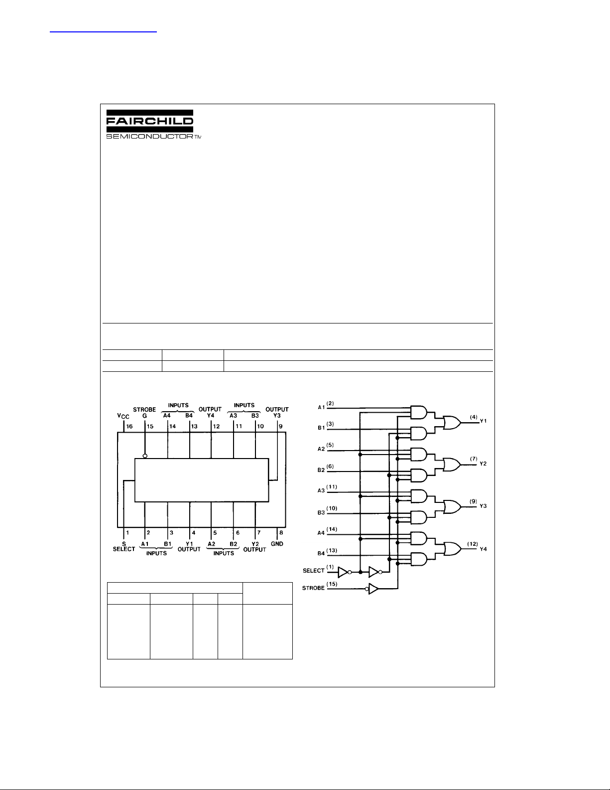
Connection Diagram
Logic Diagram
Function Table
Inputs
Strobe Select A B
HXXXL
LLLXL
LLHXH
LHXLL
LHXHH
H = HIGH Level, L = LOW Level, X = Don’t Care
© 2000 Fairchild Semiconductor Corporation DS006550 www.fairchildsemi.com
Output Y

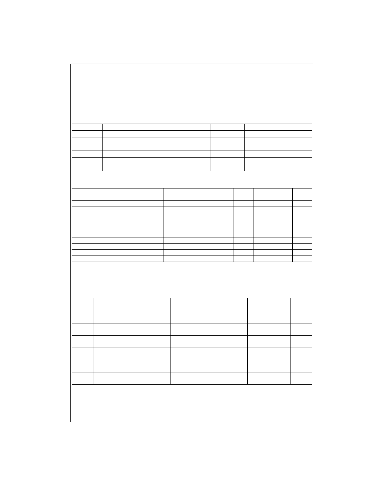
Absolute Maximum Ratings(Note 1)
Supply Voltage 7V
Input Voltage 5.5V
DM74157
Operating Free Air Temperature Range 0°C to +70°C
Note 1: The “Absolute Maximum Ratin gs” are those v alues beyon d which
the safety of the dev ice cannot be guaranteed. T he device sh ould not be
operated at these limits. The parametric values defined in the Electrical
Characteristics tables are not guaranteed at the absolute maximum ratings.
The “Recommend ed O peratin g Cond itions” t able w ill defin e the c ondit ions
for actual device operation.
Storage Temperature Range −65°C to +150°C
Recommended Operating Conditions
Symbol Parameter Min Nom Max Units
V
CC
V
IH
V
IL
I
OH
I
OL
T
A
Supply Voltage 4.75 5 5.25 V
HIGH Level Input Voltage 2 V
LOW Level In put Voltage 0.8 V
HIGH Level Output Current −0.8 mA
LOW Level Output Current 16 mA
Free Air Operating Temperature 0 70 °C
Electrical Characteristics
over recommended operating free air temperature range (unless otherwise noted)
Symbol Parameter Conditions Min
V
I
V
OH
V
OL
I
I
I
IH
I
IL
I
OS
I
CC
Note 2: All typicals are at VCC = 5V, TA = 25°C.
Note 3: Not more than one output should be shorted at a time.
Note 4: I
Input Clamp Voltage VCC = Min, II = −12 mA −1.5 V
HIGH Level VCC = Min, IOH = Max
Output Voltage VIL = Max, VIH = Min
LOW Level VCC = Min, IOL = Max
Output Voltage VIH = Min, VIL = Max
Input Current @ Max Input Voltage VCC = Max, VI = 5.5V 1 mA
HIGH Level Input Current VCC = Max, VI = 2.4V 40 µA
LOW Level Input Current VCC = Max, VI = 0.4V −1.6 mA
Short Circuit Output Current VCC = Max (Note 3) −18 −55 mA
Supply Current VCC = Max (Note 4) 30 48 mA
is measured with 4.5V applied to all inputs and all outputs OPEN.
CC
2.4 3.4 V
Typ
(Note 2)
Max Units
0.4 V
Switching Characteristics
at VCC = 5V and TA = 25°C
Symbol Parameter
t
PLH
t
PHL
t
PLH
t
PHL
t
PLH
t
PHL
www.fairchildsemi.com 2
Propagation Delay Time
LOW-to-HIGH Level Output
Propagation Delay Time
HIGH-to-LOW Level Output
Propagation Delay Time
LOW-to-HIGH Level Output
Propagation Delay Time
HIGH-to-LOW Level Output
Propagation Delay Time
LOW-to-HIGH Level Output
Propagation Delay Time
HIGH-to-LOW Level Output
From (Input) RL = 400Ω, CL = 15 pF
To (Output) Min Max
Data to Y 14 ns
Data to Y 14 ns
Strobe to Y 20 ns
Strobe to Y 21 ns
Select to Y 23 ns
Select to Y 27 ns
Units
 Loading...