Fairchild CD4049UBC, CD4050BC service manual

CD4049UBC • CD4050BC
Hex Inverting Buffer •
Hex Non-Inverting Buffer
CD4049UBC • CD4050BC Hex Inverting Buffer • Hex Non-Inverting Buffer
October 1987
Revised January 1999
General Description
The CD4049UBC and CD4050BC hex buffers are monolithic complementary MOS (CMOS) integrated ci rcu its co nstructed with N- and P-channel enhancement mode
transistors. These devices feature logic level conversion
using only one supply voltage (V
) can exceed the VDD supply voltage when these
level (V
IH
devices are used for logic level conversions. These
devices are intended for use as hex buffers, CMOS to DTL/
TTL converters, or as CMO S curre nt dr ivers, and at V
5.0V, they can drive directly two DTL/T TL loads over the
full operating temperature range.
). The input signal high
DD
Features
■ Wide supply voltage range: 3.0V to 15V
■ Direct drive to 2 TTL loads at 5.0 V over full temp erat ure
range
■ High source and sink current capability
■ Special input prote ction permits input voltages grea ter
than V
DD
Applications
=
DD
• CMOS hex inverter/buffer
• CMOS to DTL/TTL hex converter
• CMOS current “sink” or “source” dr i ver
• CMOS HIGH-to-LOW logic level converter
Ordering Code:
Order Number Package Number Package Description
CD4049UBCM M16A 16-Lead Small Outline Integrated Circuit (SOIC), JEDEC MS-012, 0.150” Narrow
CD4049UBCN N16E 16-Lead Plastic Dual-In-Line Package (PDIP), JEDEC MS-001, 0.300” Wide
CD4050BCM M16A 16-Lead Small Outline Integrated Circuit (SOIC), JEDEC MS-012, 0.150” Narrow
CD4050BCN N16E 16-Lead Plastic Dual-In-Line Package (PDIP), JEDEC MS-001, 0.300” Wide
Devices also available in Tape and Reel. Specify by appending the suffix letter “X” to the ordering code.
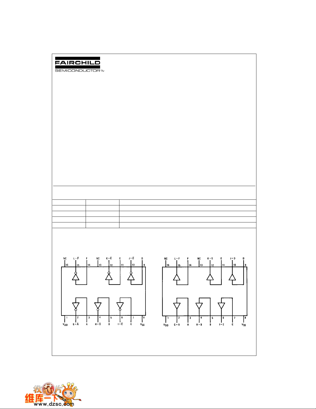
Connection Diagrams
Pin Assignments for DIP
CD4049UBC
CD4050BC
Top View
© 1999 Fairchild Semiconductor Corporation DS005971.prf www.fairchildsemi.com
Top V iew

Schematic Diagrams
CD4049UBC • CD4050BC
CD4049UBC
1 of 6 Identical Units
CD4050BC
1 of 6 Identical Units
www.fairchildsemi.com 2

Absolute Maximum Ratings(Note 1)
(Note 2)
Supply Voltage (VDD) −0.5V to +18V
Input Voltage (V
Voltage at Any Output Pin (V
Storage Temperature Range (T
Power Dissipation (P
) −0.5V to +18V
IN
)
D
) −0.5V to VDD + 0.5V
OUT
) −65°C to +150°C
S
Dual-In-Line 700 mW
Small Outline 500 mW
Lead Temperature (T
)
L
(Soldering, 10 seconds) 260°C
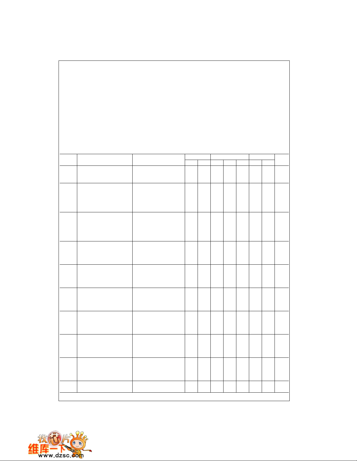
DC Electrical Characteristics (Note 3)
Symbol Parameter Conditions
I
V
V
V
V
V
V
I
I
I
Quiescent Device Current VDD = 5V 4 0.03 4.0 30 µA
DD
LOW Level Output Voltage VIH = VDD, VIL = 0V,
OL
HIGH Level Output Voltage VIH = VDD, VIL = 0V,
OH
LOW Level Input Voltage |IO| < 1 µA
IL
(CD4050BC Only) VDD = 5V, VO = 0.5V 1.5 2.25 1.5 1.5 V
LOW Level Input Voltage |IO| < 1 µA
IL
(CD4049UBC Only) VDD = 5V, VO = 4.5V 1.0 1.5 1.0 1.0 V
HIGH Level Input Voltage |IO| < 1 µA
IH
(CD4050BC Only) VDD = 5V, VO = 4.5V 3.5 3.5 2.75 3.5 V
HIGH Level Input Voltage |IO| < 1 µA
IH
(CD4049UBC Only) VDD = 5V, VO = 0.5V 4.0 4.0 3.5 4.0 V
LOW Level Output Current VIH = VDD, VIL = 0V
OL
(Note 4) VDD = 5V, VO = 0.4V 4.6 4.0 5 3.2 mA
HIGH Level Output Current VIH = VDD, VIL = 0V
OH
(Note 4) VDD = 5V, VO = 4.6V −1.0 −0.9 −1.6 −0.72 mA
Input Current VDD = 15V, VIN = 0V −0.3 −0.3 −10
IN
Note 3: VSS = 0V unless otherwise specified.
VDD = 10V 8 0.05 8.0 60 µA
VDD = 15V 16 0.07 16.0 120 µA
|IO| < 1 µA
VDD = 5V 0.05 0 0.05 0.05 V
VDD = 10V 0.05 0 0.05 0.05 V
VDD = 15V 0.05 0 0.05 0.05 V
|IO| < 1 µA
VDD = 5V 4.95 4.95 5 4.95 V
VDD = 10V 9.95 9.95 10 9.95 V
VDD = 15V 14.95 14.95 15 14.95 V
VDD = 10V, VO = 1V 3.0 4.5 3.0 3.0 V
VDD = 15V, VO = 1.5V 4.0 6.75 4.0 4.0 V
VDD = 10V, VO = 9V 2.0 2.5 2.0 2.0 V
VDD = 15V, VO = 13.5V 3.0 3.5 3 .0 3.0 V
VDD = 10V, VO = 9V 7.0 7.0 5.5 7.0 V
VDD = 15V, VO = 13.5V 11.0 11.0 8.25 11.0 V
VDD = 10V, VO = 1V 8.0 8.0 7.5 8.0 V
VDD = 15V, VO = 1.5V 12.0 12.0 11.5 12.0 V
VDD = 10V, VO = 0.5V 9.8 8.5 12 6.8 mA
VDD = 15V, VO = 1.5V 29 25 40 20 mA
VDD = 10V, VO = 9.5V −2.1 −1.9 −3.6 −1.5 mA
VDD = 15V, VO = 13.5V −7.1 −6.2 −12 −5mA
VDD = 15V, VIN = 15V 0.3 0.3 10
Recommended Operating
Conditions
Supply Voltage (V
Input Voltage (V
Voltage at Any Output Pin (V
Operating Temperature Range (TA)
CD4049UBC, CD4050BC −40°C to +85°C
Note 1: “Absolute Maximum Rat ings” are tho se values beyond which the
safety of the device cannot be guaranteed; they are not meant to imply that
the devices should be operated at these limits. The table of “Recommended Operating Conditions” and “Electrical Characteristics” provides
conditions for actual device o peration.
= 0V unless otherw is e s pecified.
Note 2: V
SS
−40°C +25°C +85°C
Min Max Min Typ Max Min Max
(Note 2)
) 3V to 15V
DD
) 0V to 15V
IN
) 0 to V
OUT
−5
−5
−1.0 µA
1.0 µA
Units
CD4049UBC • CD4050BC
DD
3 www.fairchildsemi.com
 Loading...