

CD4001BC/CD4011BC
Quad 2-Input NOR Buffered B Series Gate •
Quad 2-Input NAND Buffered B Series Gate
CD4001BC/CD401 1BC Quad 2-Input NOR Buffered B Series Gate • Quad 2-Input NAND Buffered B Series Gate
October 1987
Revised March 2002
General Description
The CD4001BC and CD4011BC quad gates are monolithic
complementary MOS (CMOS) integrated circuits constructed with N- and P-chan nel enhancement mode transistors. They have equal source and sink current
capabilities and conform to standard B series output drive.
The devices also have buffered outputs which improve
transfer characteristics by providing very high gain.
All inputs are protected against static discharge with diodes
to V
and VSS.
DD
Features
■ Low power TTL:
Fan out of 2 driving 74L compatibility: or 1 driving 74LS
■ 5V–10V–15V parametric ratings
■ Symmetrical output characteristics
■ Maximum input leakage 1
temperature range
µA at 15V over full
Ordering Code:
Order Number Package Number Package Description
CD4001BCM M14A 14-Lead Small Outline Integrated Circuit (SOIC), JEDEC MS-012, 0.150" Narrow
CD4001BCSJ M14D 14-Lead Small Outline Package (SOP), EIAJ TYPE II, 5.3mm Wide
CD4001BCN N14A 14-Lead Plastic Dual-In-Line Package (PDIP), JEDEC MS-001, 0.300" Wide
CD4011BCM M14A 14-Lead Small Outline Integrated Circuit (SOIC), JEDEC MS-012, 0.150" Narrow
CD4011BCN N14A 14-Lead Plastic Dual-In-Line Package (PDIP), JEDEC MS-001, 0.300" Wide
Devices also availab l e in Tape and Reel. Specify by appending th e s uffix let t er “X” to the ordering code.
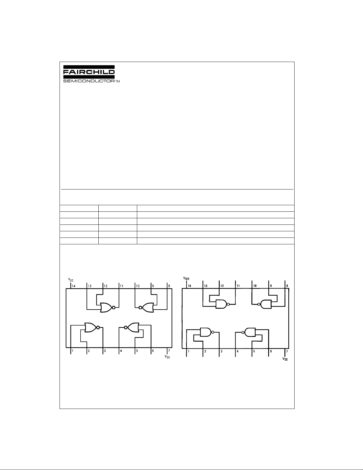
Connection Diagrams
Pin Assignments for DIP, SOIC and SOP
CD4001BC
Pin Assignments for DIP and SOIC
CD4011BC
Top View
© 2002 Fairchild Semiconductor Corporation DS005939 www.fairchildsemi.com
Top View
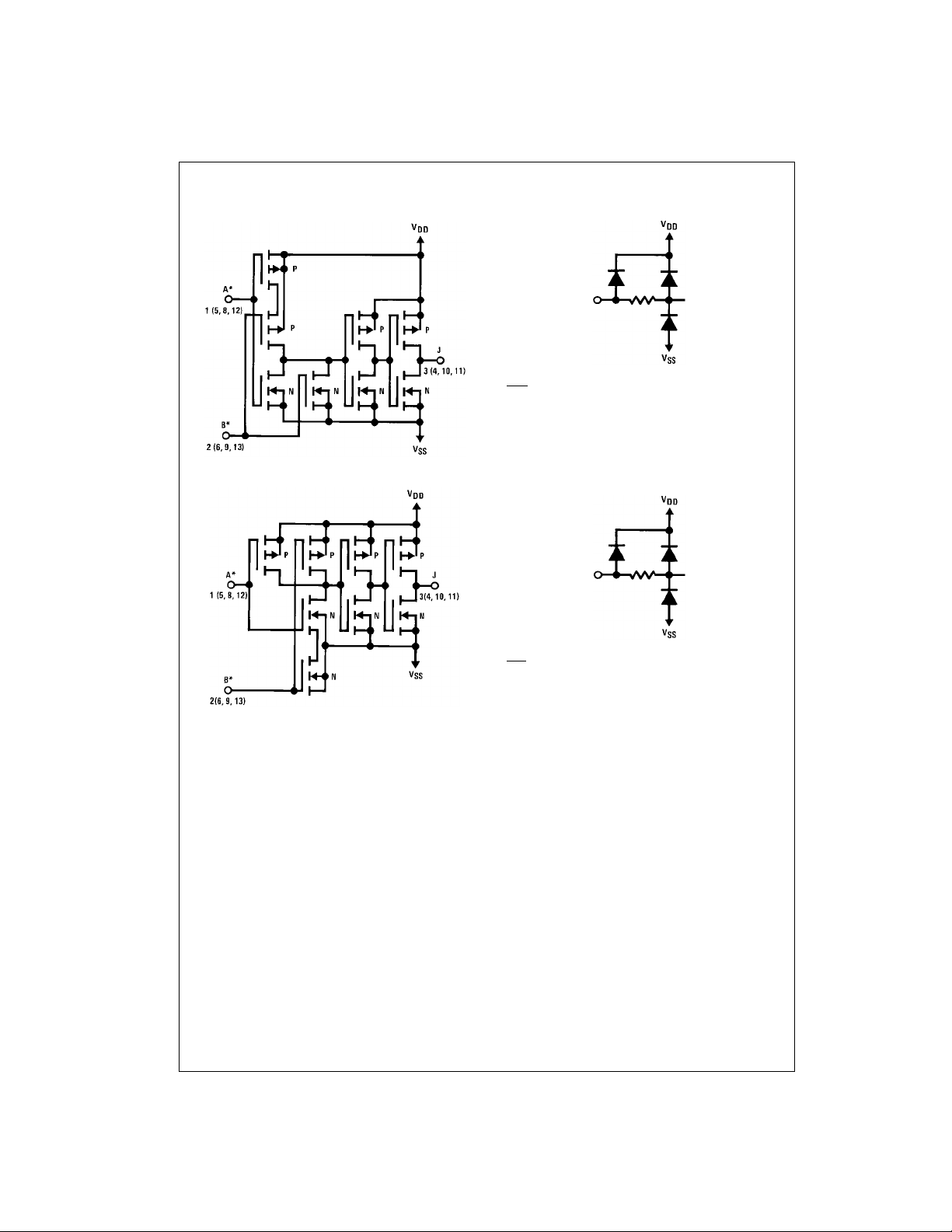
Schematic Diag r a ms
CD4001BC/CD4011BC
1
/4 of device shown
J = A + B
Logical “1” = HIGH
Logical “0” = LOW
All inputs protected by standard
CMOS protection c irc uit .
CD4001BC
CD4011BC
1
/4 of device shown
J = A • B
Logical “1” = HIGH
Logical “0” = LOW
All inputs protected by standard
CMOS protection c irc uit .
www.fairchildsemi.com 2
Absolute Maximum Ratings(Note 1)
(Note 2)
Voltage at any Pin −0.5V to VDD +0.5V
Power Dissipation (P
Dual-In-Line 700 mW
Small Outline 500 mW
V
Range −0.5 VDC to +18 V
DD
Storage Temperature (TS) −65°C to +150°C
Lead Temperature (T
(Soldering, 10 seconds) 260
)
D
)
L
Recommended Operating
Conditions
Operating Range (V
Operating Temperature Range
CD4001BC, CD4011BC
Note 1: “Absolute Maximum Ratings” are those values bey ond which the
safety of the device cannot be guaranteed. Except for “Operating T empera-
DC
ture Range” they are not meant to imply that the devic es should be operated at these limits. Th e Electrical Charact eristics tables provide conditions
for actual device operation.
Note 2: All voltages measured with respect to V
°C
fied.
)3 V
DD
DC Electrical Characteristics (Note 2)
Symbol Parameter Conditions
I
Quiescent Device VDD = 5V, VIN = VDD or V
DD
V
LOW Level VDD = 5V 0.05 0 0.05 0.05
OL
V
HIGH Level VDD = 5V 4.95 4.95 5 4.95
OH
V
LOW Level VDD = 5V, VO = 4.5V 1.5 2 1.5 1.5
IL
V
HIGH Level VDD = 5V, VO = 0.5V 3.5 3.5 3 3.5
IH
I
LOW Level Output VDD = 5V, VO = 0.4V 0.64 0.51 0.88 0.36
OL
(Note 3) V
I
HIGH Level Output VDD = 5V, VO = 4.6V −0.64 −0.51 −0.88 −0.36
OH
(Note 3) V
I
Input Current VDD = 15V, VIN = 0V −0.10 −10−5−0.10 −1.0
IN
Note 3: IOL and IOH are tested one output at a ti m e.
= 10V, VIN = VDD or V
DD
VDD = 15V, VIN = VDD or V
VDD = 15V 0.05 0 0.05 0.05
= 10V |IO| < 1 µA 9.95 9.95 10 9.95
DD
= 15V 14.95 14.95 15 14.95
V
DD
= 10V, VO = 9.0V 3.0 4 3.0 3.0
DD
= 15V, VO = 13.5V 4.0 6 4.0 4.0
V
DD
= 10V, VO = 1.0V 7.0 7.0 6 7.0
DD
= 15V, VO = 1.5V 11.0 11.0 9 11.0
V
DD
= 10V, VO = 0.5V 1.6 1.3 2.25 0.9
DD
= 15V, VO = 1.5V 4.2 3.4 8.8 2.4
DD
= 15V, VO = 13.5V −4.2 −3.4 −8.8 −2.4
DD
VDD = 15V, VIN = 15V 0.1 10−50.10 1.0
SS
SS
SS
−55°C +25°C +125°C
Min Max Min Typ Max Min Max
0.25 0.004 0.25 7.5
0.5 0.005 0.50 15
1.0 0.006 1.0 30
to 15 V
DC
−55°C to +125°C
unless otherwise speci-
SS
CD4001BC/CD4011BC
DC
Units
µACurrent V
VOutput Voltage VDD = 10V |IO| < 1 µA 0.05 0 0.05 0.05
VOutput Voltage V
VInput Voltage V
VInput Voltage V
mACurrent V
mACurrent VDD = 10V, VO = 9.5V −1.6 −1.3 −2.25 −0.9
µA
AC Electrical Characteristics (Note 4)
CD4001BC: T
Symbol Parameter Conditions Typ Max Units
t
PHL
t
PLH
t
, t
THL
C
IN
C
PD
Note 4: AC Parameters are guaranteed by DC correl at ed testing.
= 25°C, Input tr; tf = 20 ns. CL = 50 pF, R
A
Propagation Delay Time, VDD = 5V 120 250
Propagation Delay Time, VDD = 5V 110 250
Transition Time VDD = 5V 90 200
TLH
Average Input Capacitance Any Input 5 7.5 pF
Power Dissipation Capacity Any Gate 14 pF
= 200k. Typical temperature coefficient is 0.3%/°C.
L
VDD = 15V 35 70
VDD = 15V 35 70
VDD = 15V 40 80
3 www.fairchildsemi.com
nsHIGH-to-LOW Level VDD = 10V 50 100
nsLOW-to-HIGH Level VDD = 10V 50 100
nsVDD = 10V 50 100

AC Electrical Characteristics (Note 5)
CD4011BC: T
Symbol Parameter Conditions Typ Max Units
t
PHL
t
PLH
, t
t
THL
CD4001BC/CD4011BC
C
IN
C
PD
Note 5: AC Parameters are gu aranteed by DC correlated testing.
= 25°C, Input t
A
Propagation Delay, VDD = 5V 120 250
Propagation Delay, VDD = 5V 85 250
Transition Time VDD = 5V 90 200
TLH
Average Input Capacitance Any Input 5 7.5 pF
Power Dissipation Capacity Any Gate 14 pF
; tf = 20 ns. CL = 50 pF, R
r
V
V
V
= 200k. Typical Temperature Coefficient is 0.3%/°C.
L
= 15V 35 70
DD
= 15V 30 70
DD
= 15V 40 80
DD
Typical Performance Characteristics
Typical
Transfer Charact eristics
Typical
Transfer Characteristics
nsHIGH-to-LOW Level VDD = 10V 50 100
nsLOW-to-HIGH Level VDD = 10V 40 100
nsVDD = 10V 50 100
Typical
Transfer Characteristics
www.fairchildsemi.com 4
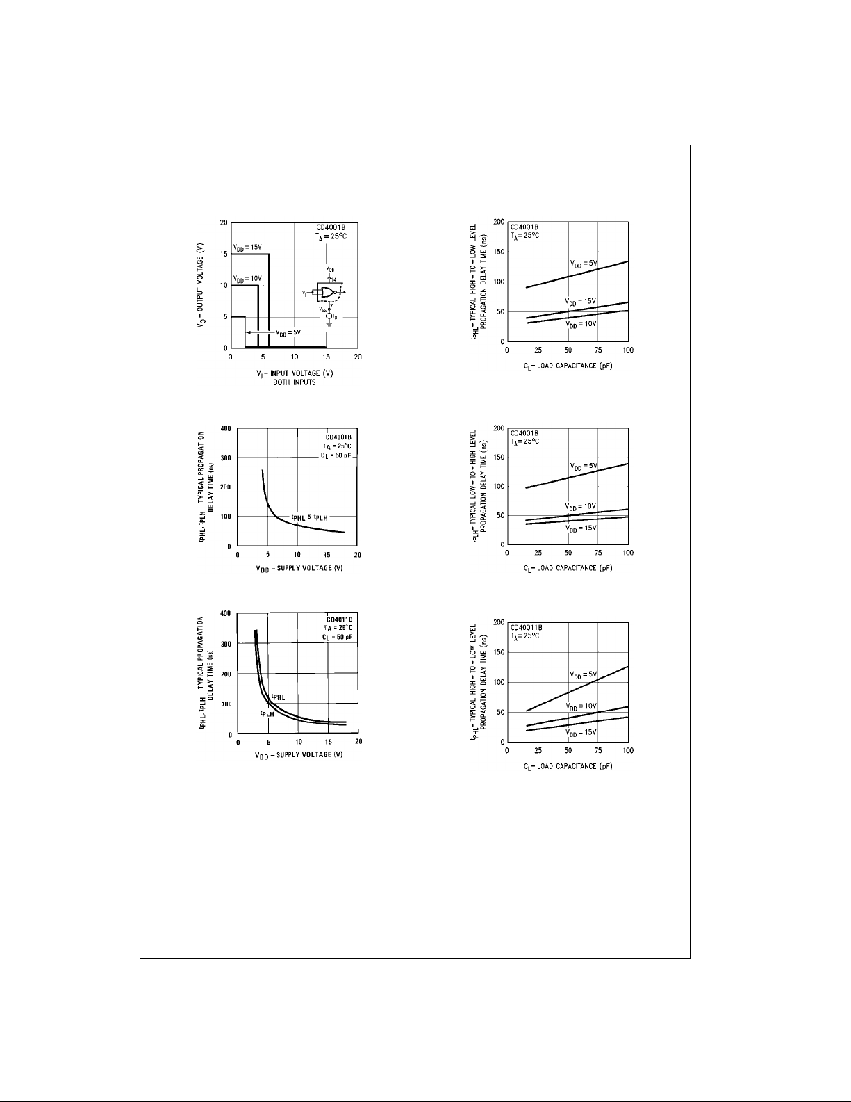
Typical Performance Characteristics (Continu ed)
Typical Transfer Characteristics
CD4001BC/CD4011BC
5 www.fairchildsemi.com

Typical Performance Characteristics (Continued)
CD4001BC/CD4011BC
www.fairchildsemi.com 6
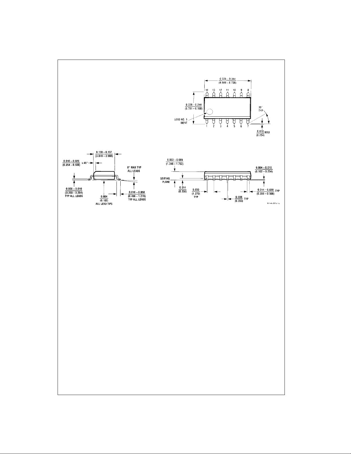
Physical Dimensions inches (millimeters) unless otherwise noted
CD4001BC/CD4011BC
14-Lead Small Outline Integrated Circuit (SOIC), JEDEC MS-012, 0.150" Narrow
Package Number M14A
7 www.fairchildsemi.com
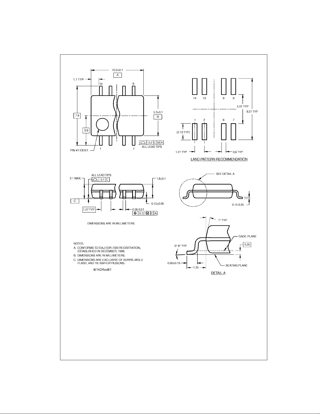
Physical Dimensions inches (millimeters) unless otherwise noted (Continued)
CD4001BC/CD4011BC
14-Lead Small Outline Package (SOP), EIAJ TYPE II, 5.3mm Wide
www.fairchildsemi.com 8
Package Number M14D

Physical Dimensions inches (millimeters) unless otherwise noted (Continued)
CD4001BC/CD401 1BC Quad 2-Input NOR Buffered B Series Gate • Quad 2-Input NAND Buffered B Series Gate
14-Lead Plastic Dual-In-Line Package (PDIP), JEDEC MS-001, 0.300" Wide
Fairchild does not assume any responsibility for use of any circuitry described , no circuit patent licenses are implied and
Fairchild reserves the right at any time without notice to change said circuitry and specifications.
LIFE SUPPORT POLICY
FAIRCHILD’S PRODUCTS ARE NOT AUTHORIZED FOR USE AS CRITICAL COMPONENTS IN LIFE SUPPORT
DEVICES OR SYSTEMS WITHOUT THE EXPRESS WRITTEN APPROVAL OF THE PRESIDENT OF FAIRCHILD
SEMICONDUCTOR CORPORATION. As used herein:
1. Life support devices or systems are dev ic es or syste ms
which, (a) are intended for surgical implant into the
body, or (b) support or sustain life, and (c) whose failure
to perform when properly used in accordance with
instructions for use provide d in the l abe ling, can be reasonably expected to result in a significant injury to the
user.
Package Number N14A
2. A critical compo nent in any com ponen t of a life s upp ort
device or system whose failure to perform can be reasonably expected to cause the failure of the life support
device or system, or to affect its safety or effectiveness.
www.fairchildsemi.com
9 www.fairchildsemi.com
 Loading...