Page 1
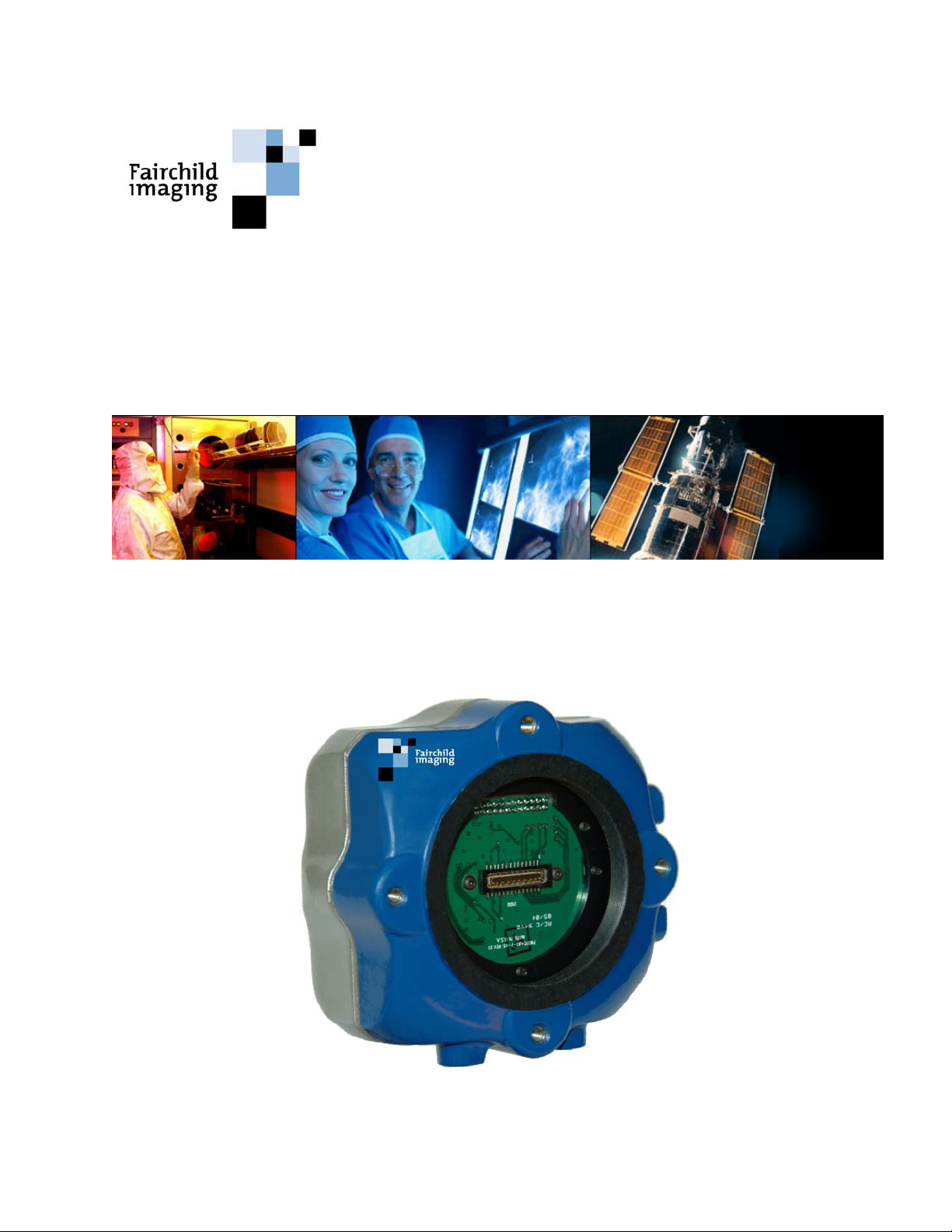
OWL CAMERA SERIES
CAM/CMOS-2K.LS
ULTRA-HIGH PERFORMANCE
Line Scan Camera
Camera User’s Manual
Models RDI & MRDI
Page 2

EMC Conformance
This equipment has been tested and found to comply with the limits for a Class A digital
device, pursuant to Part 15 of the FCC Rules.
This product fulfills the following requirements of the standards and carries the CE
marking.
EMC: FCC Part 15, Subpart B
EN 6100-6-4:2001
EN 6100-6-2:2001
EN6100-3-2:2000
EN 6100-3-3:1995/A1:2001
Fairchild Imaging • CAM/CMOS-2K.LS Line Scan Camera User’s Manual • Rev C• 2 of 42
Page 3

FAIRCHILD IMAGING
OWL CAMERA SERIES
USERS MANUAL
The CAM/CMOS-2K.LS Line Scan Camera
Rev B
© 2004 Fairchild Imaging, Inc.
Fairchild Imaging, Inc.
1801 McCarthy Blvd.
Milpitas CA 95035 USA
1-800-325-6975
www.fairchildimaging.com
PRELIMINARY DOCUMENT
The information in this manual is preliminary.
All information provided in this manual is believed to be correct at the
time of writing. No responsibility is assumed by Fairchild Imaging for its
use. Fairchild Imaging intends to make this manual as accurate as
possible and reserves the right to make changes to this information
without notice.
Terminology
Every effort has been made in this manual to use standard, consistent
definitions. In particular, the following terminology has been adopted:
TM
• Configuration refers to CameraLink
Base, Dual Base or Medium; one or two PCs; transmitted data
path width, etc.
• Mode refers to synchronization control; i.e., Freerunning, ExSynch,
etc.
• Parameter refers to user-settable variables such as exposure
(integration) time, line rate, etc.
• Environment refers to the entire collection of user-settable items:
configuration, mode, parameters, image/test pattern, etc.
setup including choice of
Fairchild Imaging • CAM/CMOS-2K.LS Line Scan Camera User’s Manual • Rev C• 3 of 42
Page 4

Table of Contents
SECTION 1
Introduction to the CAM/CMOS-2K.LS
Ultra-High Performance Line Scan Camera ........................................................ 6
1.1 Camera Highlights............................................................................................ 6
1.2 Camera Specification: RDI and MRDI Performance Specification .................. 7
1.3 Thermal Considerations ................................................................................... 8
1.4 Image Sensor................................................................................................... 9
SECTION 2
Camera Hardware Interface..................................................................................11
2.1 Installation Overview ........................................................................................11
2.2 Connectors, Pinouts and Cables ......................................................................11
2.3 Power Supply ...................................................................................................12
2.4 LED Indicator Status Lamp ..............................................................................13
SECTION 3
Camera Control .....................................................................................................14
3.1 Quick Start with the Camera Link™ Interface ..................................................14
3.2 Commands.......................................................................................................14
3.3 Camera Command Summary...........................................................................18
3.4 The Four Modes for Synchronizing with the CAM/CMOS-2K.LS .....................19
SECTION 4
Mechanical and Optical Guidance .......................................................................26
4.1 Camera Dimensions and Mounting Facilities ...................................................26
4.2 Lensing.............................................................................................................27
4.3 Lens Mount Extender Tube ..............................................................................27
4.4 Mechanical Drawing of Available Camera Face Mounting “L” Bracket.............29
4.5 Lenses..............................................................................................................30
4.6 Positioning Accuracy of the Sensor Chip in the Camera ..................................30
4.7 Illumination .......................................................................................................30
4.8 Light Sources ...................................................................................................30
4.9 Lens Modeling ..................................................................................................31
Fairchild Imaging • CAM/CMOS-2K.LS Line Scan Camera User’s Manual • Rev C• 4 of 42
Page 5

SECTION 5
Handling Instructions ...........................................................................................32
5.1 Electrostatic Discharge.....................................................................................32
5.2 Preventing ESD Damage .................................................................................32
5.3 Protecting Against Dust, Oil and Scratches......................................................32
5.4 Cleaning the Sensor Window ...........................................................................32
SECTION 6
Troubleshooting....................................................................................................33
6.1 Check the Obvious Things First .......................................................................33
6.2 Use the Camera Control Interface to Perform Checks .....................................33
6.3 Other Areas You Should Check .......................................................................33
SECTION 7
Product Support....................................................................................................35
REFERENCE A
Camera Link™ Introduction .................................................................................36
Fairchild Imaging • CAM/CMOS-2K.LS Line Scan Camera User’s Manual • Rev C• 5 of 42
Page 6

SECTION 1
Introduction to the CAM/CMOS-2K.LS
Ultra-High Performance Line Scan Camera
1.1 Camera Highlights
Description
The OWL CMOS Line Scan Camera is an ultra-sensitive camera for use in line scan applications
that demand high performance under low light conditions. The camera is based upon a 2K CMOS
linear sensor that utilizes an active reset technology to obtain high performance in low light
applications while operating at very high data rates. Two versions of this camera are available.
RDI (Read During Integration) mode runs at line rates up to 38 KHz.
Read noise for this version is ~9e- (<5.7DN in 12 bit data).
MRDI (Multiple Read During Integrate) mode has a maximum read noise
of 0.4e- at a maximum line rate of 2.9KHz.
The CMOS linear sensor that is used in this camera has a unique feature that allows gain
selectability at the pixel level. The gain of each pixel can be switched between high or low gain. In
the high gain mode, the noise is minimized, while in the low gain mode, the dynamic range is
maximized.
The 12-bit output of this camera line utilizes CameraLink and will provide data at 80 MHz (40 MHz
per output). The camera offers features such as anti-blooming and programmable gain and offset.
It is packaged in a very compacted and rugged housing that contains a standard M58 x 0.75 base
lens thread. Optional (Nikon F or C Mount) lens adapters are available.
Programmability
• Simple menu-based configuration for selection of gain, calibration, test patterns operational
control, and diagnostics.
• CameraLink
TM
camera-PC communications.
Usability
• Programmable gain, offsets, and controls
• Internal flat field correction
• Easy integration “plug compatible” Camera Link
• Exposure control
TM
interface
Fairchild Imaging • CAM/CMOS-2K.LS Line Scan Camera User’s Manual • Rev C• 6 of 42
Page 7

Full Spectrum of Applications
• Precision manufacturing inspection
• Web inspection
• Sorting and routing
• Biomedical readout systems
• Diagnostic systems
1.2 Camera Specification:
RDI and MRDI Performance Specification
Functions RDI MRDI Data rates Line rates Dynamic Range
Resolution
Pixel size
Max Clock speed
Max Pixel Clock per Output
Anti Blooming
Digitized (ADC) Output
Pixel gain selectable pixel-bypixel
Output Gain Range
External Synchronization
Random Noise (pk-pk) rms*
Noise Equivalent Exposure
Sat. Equivalent Exposure
Intuitive command-control
instruction set
Sensitivity: High gain
Low gain
Flat field correction
Lens mount type
Body Size (W H D)
Power Supply
Power Dissipation
Ambient Operating Temp
Storage Temp
Power Connector
Data Connector
Control connector
*At High Gain ** At Low Gain
Up to 80 MHz Up to 80 MHz
38 KHz 2.9 KHz
High gain 650:1
Low gain 1100:1
2048 pixels 2048 pixels
7µm x 7µm 7µm x 7µm
80 MHz 80 MHz
40 MHz 40 MHZ
15000 X 15000 X
12 bits 12 bits
1X or 8.5X 1X or 8.5X
18 dB 18 dB
Option available Option available
44DN pk-pk, 6DN RMS 3DN pk-pk, 0.4DN RMS
9.7 pJ/CM
5 nJ/CM
See Section 3.2 See Section 3.2
>700 DN/nJ/cm2
61.5 DN/nJ/cm2
Internal Internal
M58 to Nikon F-mount &
C – mount
3.92” W x 3.92”H x 1.84 D 3.92” W x 3.92”H x 1.84 D
5.0V 5.0V
2.5W 2.5W
0 to 45° C 0 to 45° C
0 to 75° C 0 to 75° C
4 – pin Hirose HR10A-7R-4P 4 – pin Hirose HR10A-7R-4P
MDR-26 CameraLinkTM config.
Single Base
One 3m 10226-6212VC
CameraLinkTM Connectors CameraLinkTM Connectors
Table 1.2.1
High gain 10,000:1
Low gain 31,000:1
2 *
.7 pJ/CM2
2 *
40 nJ/CM
2**
5 nJ/CM
>700 DN/nJ/cm2
61.5 DN/nJ/cm2
M58 to Nikon F-mount &
C-mount
MDR-26 CameraLinkTM config.
Single Base
One 3m 10226-6212VC
2
40 nJ/CM
2**
Fairchild Imaging • CAM/CMOS-2K.LS Line Scan Camera User’s Manual • Rev C• 7 of 42
Page 8

Function Factory
Reset to Default Conditions X X
Fixed Pattern Noise Correction X X X
PRNU Correction X X
Integration Time X X
External Synch / Free Run X X
Pixel Level Gain X X
Line Synchronization X X
Test Patterns X X X
1.3 Thermal Considerations
The CAM/CMOS 2K.LS has been carefully designed to separate the camera electronics
from the image sensor. In addition, the Fairchild Imaging CMOS sensor runs cooler than a
CCD device
.
Table 1.2.2
Settings and Controls
Calibrated
User
Settable
Camera
Link
Fairchild Imaging advises waiting until the camera has stabilized
thermally before performing offset and gain corrections. You can determine
that the camera has stabilized thermally by repeatedly using the "TSB"
command to read sensor temperature. When sensor temperature changes
less than 0.1
°
C per minute, the camera has stabilized.
Try to avoid excess temperatures in the ambient around the camera.
Fairchild Imaging • CAM/CMOS-2K.LS Line Scan Camera User’s Manual • Rev C• 8 of 42
Page 9
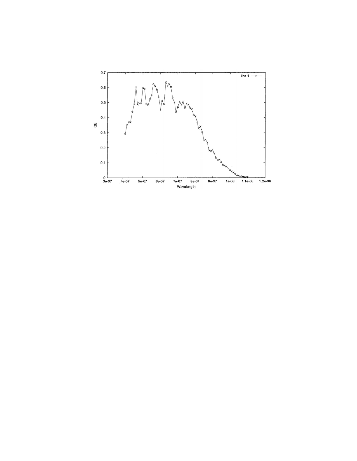
1.4 Image Sensor
Figure 1.3.1
RDI and MRDI Responsivity Curve
Pixel level processing image sensors are based on the principle that photons induced by charge at
the pixel site should be converted to, as nearly as possible, a noise-free signal at the pixel site.
The application of this principle produces the lowest possible noise and also allows signal control
at each pixel.
As is true in other sensors, photons induce charge which is collected on a capacitor at the photo
site. In a pixel level processing sensor, this charge is converted to an amplified voltage at the
pixel. This voltage is then read out through a multiplexor to an external circuit. Since the readout
starts with a strong signal, the dominant read noise source is the noise associated with the charge
accumulation at the pixel.
The 2048 x 1 linear CMOS image sensor uses a low fixed pattern noise capacitive transimpedance
amplifier (LFPN CTIA) pixel architecture. The pixel also includes circuitry for reducing 1/f noise,
correlated double sampling, electronic shuttering, and a horizontal anti-blooming drain. High speed
non-destructive readout of the sensor is achieved by using a hierarchial readout structure with two
output ports.
In simplified form, the pixel integration cycle consists of three steps: 1) reset the capacitor to fully
charged, 2) accumulate electrons on the capacitor, and 3) read the resulting charge value.
Conventionally these steps have been done by sensor-wide controls. Use of pixel level processing
results in at least an order of magnitude reduction in noise due to the reset step as well as noise
reduction in the multiplexing of the pixel values and the noise due to amplification for off chip drive.
Shown on the following page is a block diagram of the Fairchild Imaging 2048 x 1 CMOS sensor.
Fairchild Imaging • CAM/CMOS-2K.LS Line Scan Camera User’s Manual • Rev C• 9 of 42
Page 10
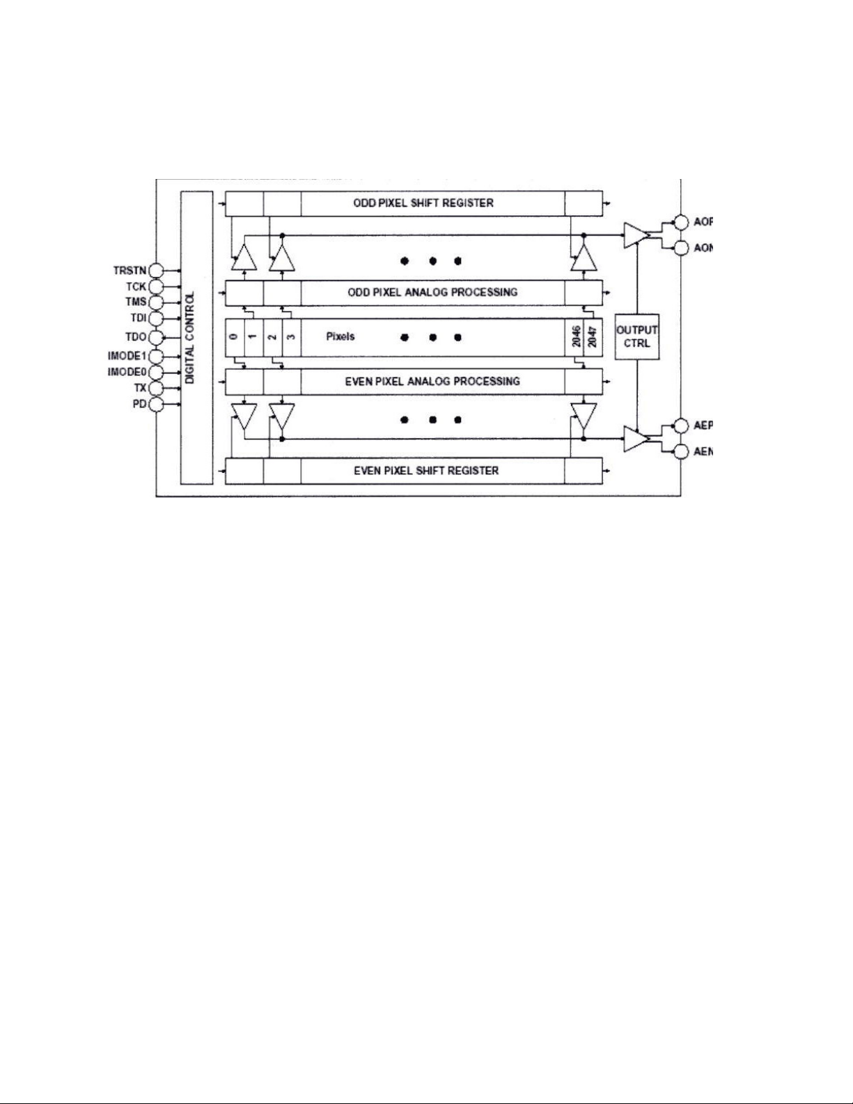
Figure 1.4.1
Fairchild Imaging • CAM/CMOS-2K.LS Line Scan Camera User’s Manual • Rev C• 10 of 42
Page 11
SECTION 2
Camera Hardware Interface
2.1 Installation Overview
Before you integrate your camera into your system you should first determine some basic
operating parameters such as what resolution you need. Do you know the speed of the object that
your camera will be inspecting? One additional point you want to keep in mind is your lighting
requirement.
One major item that you should identify early on in developing your system is the source of your
EXSYNC control signal ( framegrabber, custom controller, shaft/web encoder, etc.).
2.2 Connectors, Pinouts, and Cables
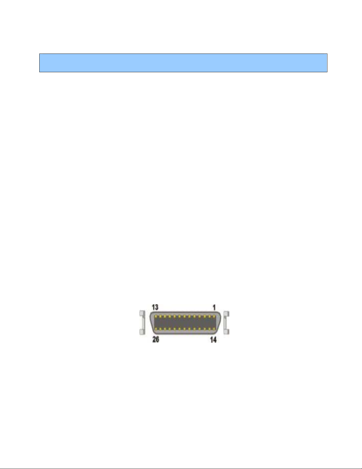
The CAM/CMOS-2K.LS uses one MDR-26 connector for CameraLink TM to communicate control
signals, data signals, and serial communications.
TM
CameraLink
and others, so that detailed cabling work is unnecessary.
cables are available as a standard off-the-shelf-part, 3M #14X26-SZLB-XXX-OLC
Figure 2.2.1
MDR-26 CameraLink
3M p/n 334 – 34 series
TM
Connector
Fairchild Imaging • CAM/CMOS-2K.LS Line Scan Camera User’s Manual • Rev C• 11 of 42
Page 12

Table 2.2.1
Camera Pin # Frame Grabber Pin # Channel Link Signal
1 1 Inner shield
14 14 Inner shield
2 25 X0
15 12 X0+
3 24.0 X1-
16 11 X1+
4 23 X2-
17 10 X2+
5 22 Xclk
18 9 Xclk+
6 21 X3
19 8 X3+
7 20 SerTC+
20 7 SerTC-
8 19 SerTFG-
21 6 SerTFG+
9 18 CC1-
22 5 CC1+
10 17 CC2-
23 4 CC2+
11 16 CC3-
24 3 CC3+
12 15 CC4-
25 2 CC4+
13 13 Inner shield
26 26 Inner shield
Notes:
• Exterior overshield is connected to the shells of the connectors on both ends.
• 3M part 14X26-SZLB-XXX-0LC is a complete cable assembly, including connectors.
• Unused pairs should be terminated in 100 ohms at both ends of the cable.
2.3 Power Supply
• The camera uses a single voltage input, normally set to 5.0V.
• Ripple and noise is required to be < 20 mV RMS.
• Power is supplied through a Hirose connector.
• When installing the mating connector, be sure to line up the slots. This action will assure that
you will not bend any of the pins.
Fairchild Imaging • CAM/CMOS-2K.LS Line Scan Camera User’s Manual • Rev C• 12 of 42
Page 13
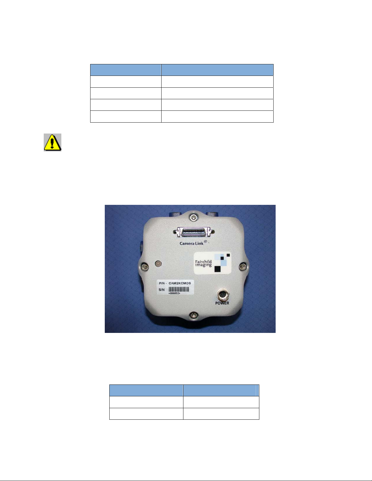
Table 2.3.1
Hirose Receptacle
Pin # Description
1 +5.0 - +6.0 V DC
2 +5.0 – +6.0V DC
3 Ground
4 Ground
If you are using an adjustable lab power supply it is extremely important that
you apply the apppropriate voltage to your camera. Incorrect voltage might damage
the camera.
Figure 2.3.1
Back View of CAM/CMOS – 2K.LS
2.4 LED Indicator Status Lamp
Table 2.4.1
Light Color Status
Green Running
Blinking Amber/Red Busy with command
Fairchild Imaging • CAM/CMOS-2K.LS Line Scan Camera User’s Manual • Rev C• 13 of 42
Page 14

SECTION 3
Camera Control
3.1 Quick Start with the Camera LinkTM Interface
Follow your Frame Grabber manufacturer’s instructions when inserting the frame grabber card into
your PC. Be sure that you install the correct configuration software that matches the camera that
you are using.
At this point your camera should already be connected to the DC power supply, and connected to
the frame grabber in your PC. Your frame grabber will see our camera and start communicating
almost immediately. As soon as your camera starts communicating with the frame grabber, you
can verify this fact by looking at your monitor and observing the video signal.
To communicate with your camera we have created specific commands. In the next section we will
go over these commands in detail.
3.2 Commands
Note: Commands are not case sensitive. To input commands, type in the three character
command and hit enter.
Command Syntax:
Command + enter, example: Type in RSH, then enter
Command + enter + value, example: Type in SSM then enter, then type 2
Command + enter + value + enter, example: Type in SLR then enter, then type 2000, then enter
RSH
This command allows you to perform a hard camera reboot.
The camera returns….………..…Reboot Started
RSS
This command allows you to perform a logic reset.
No return………………………….no message
INQ
This command will show you what camera is connected to your PC.
The camera returns…..………….Fairchild Imaging 2K CMOS
Fairchild Imaging • CAM/CMOS-2K.LS Line Scan Camera User’s Manual • Rev C• 14 of 42
Page 15

VER
This command will show you the current software version in your camera.
The camera returns………………...FPGA REV.2.5 The current value may be different
Micro rev. 0.90
Prod rev. A 1.01
SLR
This command allows you to set line rate, enter value and enter.
The range for line rate should be 204 – 38610.
CPO
This command allows you to Calibrate Pixel Offset. You can observe this command by the
blinking green/amber LED. When the LED stops blinking, that means that the calibration of the
pixels is completed.
You must cover lens when performing this operation!
CPG
This command allows you to Calibrate Pixel Gain. We strongly recommend that this command
be done after each CPO. To perform this operation correctly the camera must look at a
uniform illuminated light source. The LED will be a blinking amber/red.
VOM
This command reads the different component voltages located within the camera.
The camera returns…………………INPUT = 6.103
3.9VD = 3.225
3.4VS = 3.448
1.5VD = 1.495
1VAD2 = 0.980
1VAD = 0.980
TSB
This command reads the internal camera temperature.
The camera returns…………………Temp 39.42°C (example)
SIT
This command allows you to set the integration time.
Set line rate first (SLR) before using this command.
Enter value plus enter value in microseconds, Range is 20 – 4900.
Fairchild Imaging • CAM/CMOS-2K.LS Line Scan Camera User’s Manual • Rev C• 15 of 42
Page 16

SSM
This command allows you to set the Sync mode. When selecting the option you need, enter
the appropriate single digit number, and then hit enter.
Value
Function
The camera returns …………..…..1 Free run
2 External Sync
3 External Sync, fixed integration
4 External Sync, electronic shutter
SCM
This command allows you to select a correction mode. When selecting the option you need,
enter the appropriate single digit number and then hit enter.
Value
The camera returns……………….1 M1 (1
2 M2 (2
Function
st
memory)
nd
memory)
3 Offset Correction
4 Gain Correction
5 No Correction
6 Full Correction
STP
This command allows you to select a test pattern. When selecting the option you need, enter the
appropriate single digit number, and then hit enter.
Value
Function
No output from camera…………1 Horizontal Ramp
2 Vertical Ramp
3 Vertical Bars
4 Vertical Ramp and Bars
5 0
6 4095
Other Video
CBR
This command allows you to change the Baud Rate. You will not see anything on your
monitor.
Here is a table of stored rates in the camera…Value
Function
1 9600
2 19200
3 38400 (Default)
4 57600
5 115200
If you can’t resist changing the baud rate, select the appropriate single digit number and hit
enter.
Fairchild Imaging • CAM/CMOS-2K.LS Line Scan Camera User’s Manual • Rev C• 16 of 42
Page 17

LED
This command allows you to change the color. When selecting the option you need to, enter
the appropriate single digit number and hit enter. Your screen will be blank during this
command
You can input one of the following:
Value
Function
0 Amber
1 Green
2 Red
3 Off
GDA
This command allows you to show all of the DACs (Digital to Analog Converter). When
selecting the option you need, enter the appropriate single digit number and hit enter.
The camera returns…
3:Gain F_odd = 0.490V 8:GainF_even = 0.490V
2:GainC_odd = 0.235V 6:GainC_even = 0.235V
4:Offset_odd = 1.199V 7:Offset_even = 1.199
1:CML_odd = 1.425V 5:CML_even = 1.425
SDN
This command allows you to select one of the above DAC numbers, and change its value.
Example: SDN + enter + 486 + enter enter value between 0 - 1023
GDN
This command allows you to verify what you just did under the SDN command.
Example: you would input the following GDN + enter + 1
The camera returns a value between 0 - 1023
SAP
Store in Flash both correction memories, all registers and DAC values.
Value
Function
Store all parameters 0 Default factory calibrate
1 User
2 User
RAP
Load from flash to camera. Recall all parameters.
Value
Function
0 Default factory calibration
1 User
2 User
Fairchild Imaging • CAM/CMOS-2K.LS Line Scan Camera User’s Manual • Rev C• 17 of 42
Page 18

SBS
Value
Function
Set bit shift 0 12 bit
1 10 bit
2 8 bit
CAO
Adjust analog video offset mismatch. Calibrate analog offset 200 DN.
SAG
Set analog gain 0 – 10 db
CAG
Adjust analog video gain mismatch. Calibrate analog gain.
GSN
Get camera serial number, returns 128 character string: serial number, model, etc.
SGH
Set gain high. Set pixel gain in sensor.
SGL
Set gain low. Set pixel gain in sensor.
3.3 Camera Command Summary
Command Definition Summary
RSH Reboot System Hard Hard reboot of camera
RSS Reset Command Logic reset of camera
INQ Inquiry Shows what camera is used
VER Version Shows current software
SLR Set Line Rate This function allows line rate change
CPO Calibrate Pixel Offset This function performs correction of pixel
CPG Calibrate Pixel gain This function performs correction of pixel
VOM Voltage monitoring This function shows internal voltages
TSB Temperature Sensor Board This function shows temp. of sensor board
SIT Set Integration Time This function allows user to set integration
SSM Set Sync Mode This function allows user to select sync
SCM Select Correction Mode This function allows user to select
STP Select Test Pattern This function allows user to select test
Table 3.3.1
offset
gain
time
mode
correction mode
pattern
Fairchild Imaging • CAM/CMOS-2K.LS Line Scan Camera User’s Manual • Rev C• 18 of 42
Page 19

Command Definition Summary
CBR Change Baud rate This function allows user to select baud
rate
LED Light Emitting Diode Change LED state
GDA Get DAC All Returns current DAC setting as a voltage
SDN Set DAC number Change DAC (n) value
GDN Get DAC number Get DAC (n) value
SBS
SAP
RAP
GSN
CAO
CAG
SAG
SGH Set Gain High Set Pixel gain in Sensor
SGL Set Gain Low Set Pixel gain in Sensor
Set Bit shift This function allows user to shift 12, 10, 8
bit video
Stores all parameters This function allows you to save default or
user settings
Recalls all parameters This function allows user to recall the
factory calibration
Get serial number This function allows user to retrieve
camera info, e.g., model + camera serial
number
Calibrate Analog Offset This function allows user to calibrate the
analog offset
Calibrate Analog Gain This function allows user to calibrate the
analog Gain
Set Analog Gain This function allows user to set the analog
gain
3.4 The Four Modes for Synchronizing with the CAM/CMOS – 2K.LS
There are four synchronization modes as explained below and summarized in Table 3.4.1 below.
Freerunning Mode is described below in (Figure 3.4.2). In this mode, the camera is not triggered;
instead it drives the world around it. It is the default mode set and shipped by the factory.
ExSync Line Synchronization is described below (Figure 3.4.3). The target asychronously
synchronizes the CAM/CMOS – 2K.LS from an external trigger via the ExSync line. The user
selects ExSync Synchronization or any of the modes via the camera command set. In this mode,
start of integration is asynchronously controllable with ExSync, and continues until the end of the
line period.
ExSync Line Synchronization with Programmable Integration Time is described in (Figure
3.4.4). This mode is similar to ExSync Synchronization, but in addition, in this mode the user can
program the duration of integration over the serial interface to be less than to the end of the line
period.
Fairchild Imaging • CAM/CMOS-2K.LS Line Scan Camera User’s Manual • Rev C• 19 of 42
Page 20

ExSync Line Synchronization with Electronic Shutter Control is the fourth mode (Figure 3.4.5).
It gives the user asynchronous hardware control both start and end of integration.
TM
The control lines ExSync and ElectronicShutter are CameraLink
lines CC1 and CC2 respectively
as described in Reference A, and must be asserted by the frame grabber.
Mode
Synchronization
1
Free
Running
(factory default)
The CAM/CMOS
2K.LS drives the frame
grabber(s).
Motion of the subject
being imaged must be
synchronized to the
CAM/CMOS-2K.LS
.
2
ExSynch
Sychronization
ExSynch
Synchronization
3
Programmable
Integration Time
ExSynch
Synchronization
4
Electronic
with
with
Shutter
Control
The User
Synchronizes
the
CAM/CMOS-2K.LS
via an
Encoder.
Summary of CAM/CMOS-2K.LS Modes
Line
Start
Trigger
The
CAM/CMOS -
2K.LS
LineValid
Camera
Output
Triggers
the
frame
grabber(s)
by
Going
High
The
User
Triggers
the
CAM/CMOS-
2K.LS
by
taking
ExSynch
Camera
Input
Low
Table 3.4.1
Line
End
Line Ends
- t
t
LinePeriod
LineValid
Camera Output
Goes High
User may set
with Software
When the User
Camera Input Low
(In this way,
Line Rate
User-Set
Frequency
ExSynch)
after
t
LinePeriod
takes
ExSynch
Again
the
is
by
of
XFR
Start
of
Integration
t
Initiatio n
+ t
Reset
-t
XFR
after
LineValid
Camera Output
Goes High
t
Reset
after
the System
takes
the
ExSynch
Camera Input
High
t
Reset
after
the User
takes
ElectronicShutter
Camera Input High
End
of
Integration
t
Integration
after
start of Integration
User may set
t
Integration
with Software
When the User
takes
ExSynch
Camera Input Low
+ t
t
Integration
after User
takes ExSync
Camera Input High
ElecShutter
Camera Input Low
Reset
When
the User
takes the
Fairchild Imaging • CAM/CMOS-2K.LS Line Scan Camera User’s Manual • Rev C• 20 of 42
Page 21

Figure 3.4.1 -- Mode 1: Freerunning
...in this basic mode, usually used for diagnostics & debugging,
no triggering is applied to the camera...
...instead, the camera drives the system with the LineValid Camera Output.
The Line Period and Integration
t
LinePeriod
n
t
t
Initiation
Reset
t
IntegrationMax
may be shortened
with the Command Software
LineValid
Camera Output
t
Notes specific to this mode
1 The camera is not triggered -- instead, the camera itself synchronizes the system. This is the default mode
set by the factory
The camera internally initiates readout of line "n" on its own. LineValid goes high a time "t
2
3 The user must synchronize motion of the material moving past the camera to the camera's LineValid output
4 The user must synchronize collection of data in the PC frame grabber to the LineValid camera output
5 While LineValid is high, data may be sampled on rising edges of Camera Strobe Output for the 2048 clock cycles
of readout as shown in the inset above; this is the same for all four modes
A time "t
6
initiates pixel reset; Integration then begins time "tReset" later, with this integrated information to be read out
in the subsequent line "n+1"
7 The factory-set default is for integration to run until the end of the line period, which results in a maximum
integration time "t
The line period "t
8
" after the camera internally initiates the readout-and-integration cycle, the camera also internally
Initiation
XFR
2048 Clock Cycles
IntegrationMax
LinePeri od
" = "t
" and the integration time "t
t
Readout
LinePeri od
Data Came ra Outpu t
Strobe Cam era Output
Line Va lid Came ra Output
" - "t
Reset
1 2 3 1023 1024
" afterwards
XFR
" - "t
Integration
".
Initiation
" are selected by the user with the Command Software
n+1
Fairchild Imaging • CAM/CMOS-2K.LS Line Scan Camera User’s Manual • Rev C• 21 of 42
Page 22

c
Figure 3.4.2 -- Mode 2: ExSync Synchronization
...gives the user asynchronous hardware control over initiation of the camera readout cycle
and over termination of the line period...
...separately gives the user asynchronous hardware control
ExSyn
Camera Input
LineValid
Camera Output
>t
MinS ync
n
t
Reset2
t
Hold
t
Readout
2048 Clock Cycles
t
XFR
t
LinePeriod
Dat a Ca m er a O utpu t
Strobe Came ra Output
t
Integration
1 2 3 1023 1024
Notes specific to this mode
1
Unlike Freerunning mode, the user triggers (separately) both the CAM/CMOS - 2K.LS readout cycle, and the CAM/CMOS - 2K.LS
reset-&-integration cycle. All of the modes other than Freerunning mode allow the user to do this
2 The user initiates a readout cycle by taking ExSync low as shown above. Readout actually begins a time
" after ExSync is taken low, and lasts 2048 clock cycles
"t
XFR
3 The user can read data from the CAM/CMOS - 2K.LS while LineValid is high as shown above and explained in Figure 3.4.1
4 The reset-&-integration cycle to be read out in the next period "n+1" is initiated by ExSync returning high;
integration begins when reset is complete a time "t
for the remainder of "t
5 The line period is set by the user by returning ExSync low, thereby initiating the next "n+1th" readout cycle
The minimum time that ExSync can be held low is "t
6
7 Integration is cut off when the user takes ExSync low again as shown in the waveforms above
The line period must be greater than or equal to "t
8
9 If the user brings the ExSync Camera Input low prior to "tXFR" + "tReadout" after ExSync goes low, then the CAM/CMOS
2K.LS delays initiation of the "n+1th" readout cycle until "t
". The user can therefore shorten integration time by increasing "t
LinePeriod
Line Va lid Cam era Output
" after ExSync goes high, and continues
Reset
" as shown above
MinSync
plus t
Readout"
", which sets maximum line rate to 50K lines/sec
Xfr
"+ "t
Readout
" has elapsed after ExSync last went low
XFR
Hold
" above
n+1
Fairchild Imaging • CAM/CMOS-2K.LS Line Scan Camera User’s Manual • Rev C• 22 of 42
Page 23

c
Figure 3.4.3 -- Mode 3: ExSync Synchronization with Programmable Integration Time
...Mode 3 is similar to Mode 2...
...the differences are that the reset-&-integration cycle is initiated when ExSync is taken low...
...and the duration of integration
Ex
Syn
C
amera Input
n
t
Reset3
user-set with command software
t
HoldLow
>t
MinS ync
t
Integration
t
LinePeriod
t
HoldHigh
>t
Setup
n+1
LineValid
C
amera Output
t
t
XFR
Notes specific to this mode
1 The reset-and-integration cycle is initiated by ExSync being taken low by the user; this has the effect
of starting integration as soon as possible at the beginning of the line period
ExSync must be returned high at least "t
2
The user sets integration time "t
3
4 The user can read data from the CAM/CMOS - 2K.LS while LineValid is high as shown above.
Readout
2048 Clock Cycles
" with the software command set
Integration
Data Came ra Output
1 2 3 1023 1024
Strobe Came ra Output
Line Valid Camera Output
" prior to taking it low again to signal the end of the line period
Setup
Fairchild Imaging • CAM/CMOS-2K.LS Line Scan Camera User’s Manual • Rev C• 23 of 42
Page 24

y
Figure 3.4.4 -- Mode 4: ExSync Synchronization and Electronic Shutter Control
...this mode gives the user full asynchronous hardware control over start and end of integration
with the "ElectShutter" Camera Input.
t
LinePeriod
n
ElectShutter
Camera Input
t
Wait
>t
x2p
ExSync
Camera Input
LineValid
Camera Output
2048 Clock Cycles
t
XFR
Notes specific to this mode
1 The user initiates the reset-&-integration cycle by taking the ElectShutter Camera Input high
2 The user terminates integration by taking the ElectShutter Camera Input low
ElectShutter will not be recognized by the camera until a time "t
3
4 If ElectShutter is brought high earlier than constrained above, the camera will interpret this as ElectShutter
going high "t
5 Any software command setting integration time is overridden by ElectShutter Camera Input
6 If ElectShutter is still high when ExSync is taken low to initiate the next readout cycle, then integration is
immediatel
7 The user can read data from the CAM/CMOS - 2K.LS while LineValid is high as shown above.
" after ExSync went high
x2p
terminated
t
>t
MinSync
t
Readout
HoldLow
t
Reset
Da ta C am era Ou tput
Strobe Ca me ra Output
Line Va lid Came ra Output
t
Integration
t
HoldHigh
>t
1 2 3 1023 1024
" after ExSync is brought low
x2p
Setup
n+1
Fairchild Imaging • CAM/CMOS-2K.LS Line Scan Camera User’s Manual • Rev C• 24 of 42
Page 25

Table 3.5.6
Synchronization Timing Values
CAM/CMOS-2K.LS
t
XFR
t
initiation
t
Readout
t
Reset2
t
Reset3
300nsec
40nsec
25.6nsec
4µsec
5µsec
t
MinSynch
t
t
Hold
x2p
1.425µsec
1.425µsec
875ns
Fairchild Imaging • CAM/CMOS-2K.LS Line Scan Camera User’s Manual • Rev C• 25 of 42
Page 26
SECTION 4
Mechanical and Optical Guidance
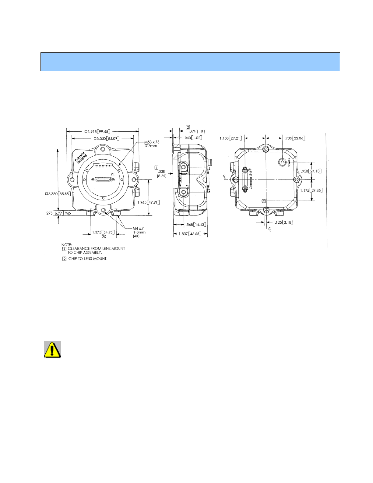
Figure 4.1
4.1 Camera Dimensions and Mounting Facilities
The CAM/CMOS – 2K.LS camera housing is manufactured with high precision. Planar, parallel,
and angular sides guarantee precise mounting with high repeatability.
The CAM/CMOS – 2K.LS is equipped with four M4 mounting holes on the front and two M4
mounting holes on one side and on the bottom of the camera.
Use caution in the following ways to avoid stripping threads or stressing the
case:
• Use only M4 screws -- do not try other metric approximation size screws
• Do not over torque; do not over tighten screws beyond the depth of the holes; do not otherwise
force screws or create a bending moment with them
• Use caution in crafting mounting brackets so that you do not interfere with the lens, or exert
force on the lens extender tube barrel, or torque or otherwise place force on any of the
connectors on the back of the case. A "L" mounting bracket (figure 4.4) is available; contact
your Fairchild Imaging representative for more details.
Fairchild Imaging • CAM/CMOS-2K.LS Line Scan Camera User’s Manual • Rev C• 26 of 42
Page 27
4.2 Lensing
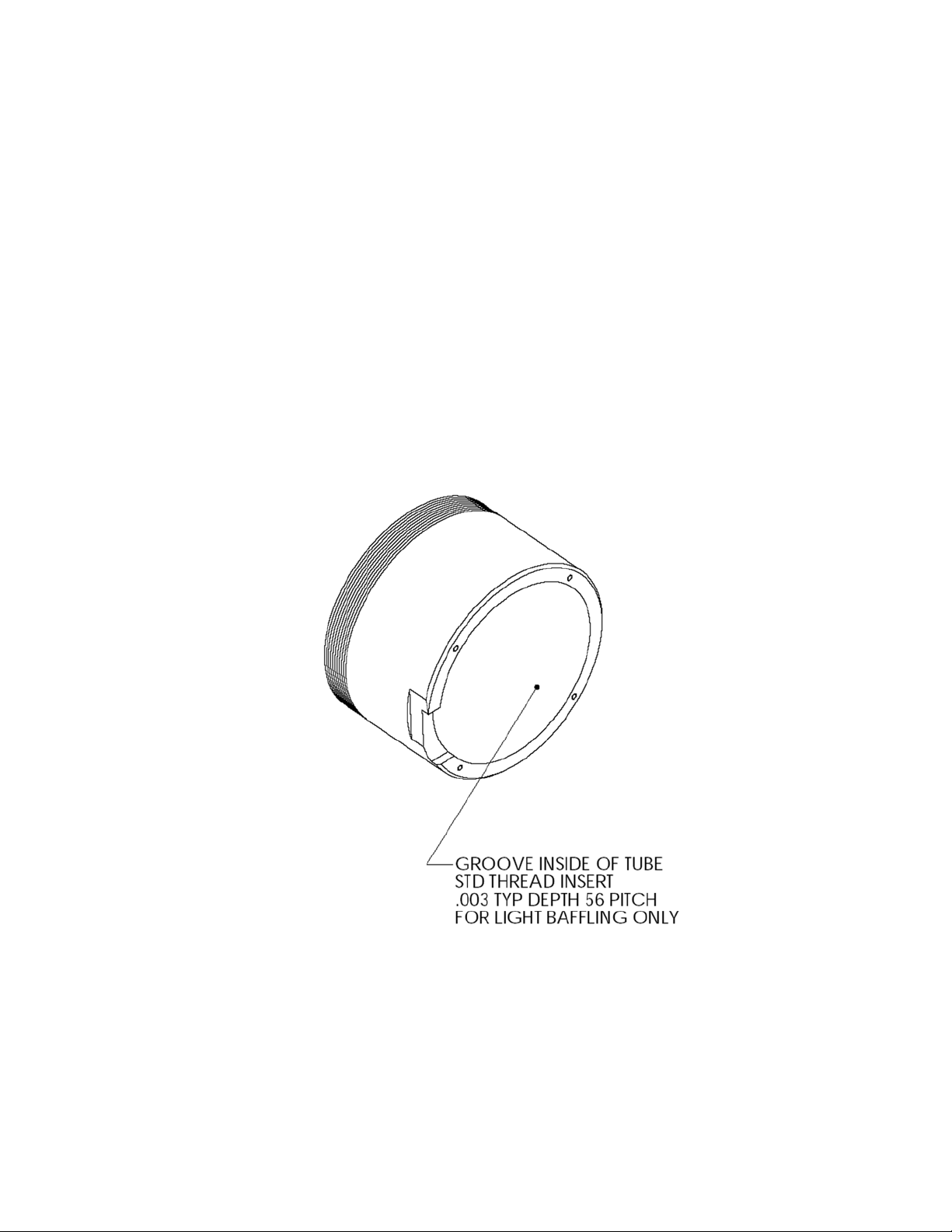
The CAM/CMOS – 2K.LS as shipped from the factory accepts universal manual "F" mount lenses
that are available from a number of suppliers. The standard 0.050" Nikon mounting ring is shown in
Figure 4.3 below.
Figure 4.3 below shows that the lens extender tube can be detached by unscrewing it so that an
optional "C" mount can be installed. If you wish to do this, please contact your Fairchild Imaging
Sales representative.
With the lens mount (lens extender tube and its lockring) removed, the front surface of the camera
is seen as a square with a large threaded hole in the center. The "z" distance from the surface of
the square to the top of the sensor is 13.72mm.
4.3 Lens Mount Extender Tube
Figure 4.3.1
Fairchild Imaging • CAM/CMOS-2K.LS Line Scan Camera User’s Manual • Rev C• 27 of 42
Page 28

Figure 4.3.2
Fairchild Imaging • CAM/CMOS-2K.LS Line Scan Camera User’s Manual • Rev C• 28 of 42
Page 29
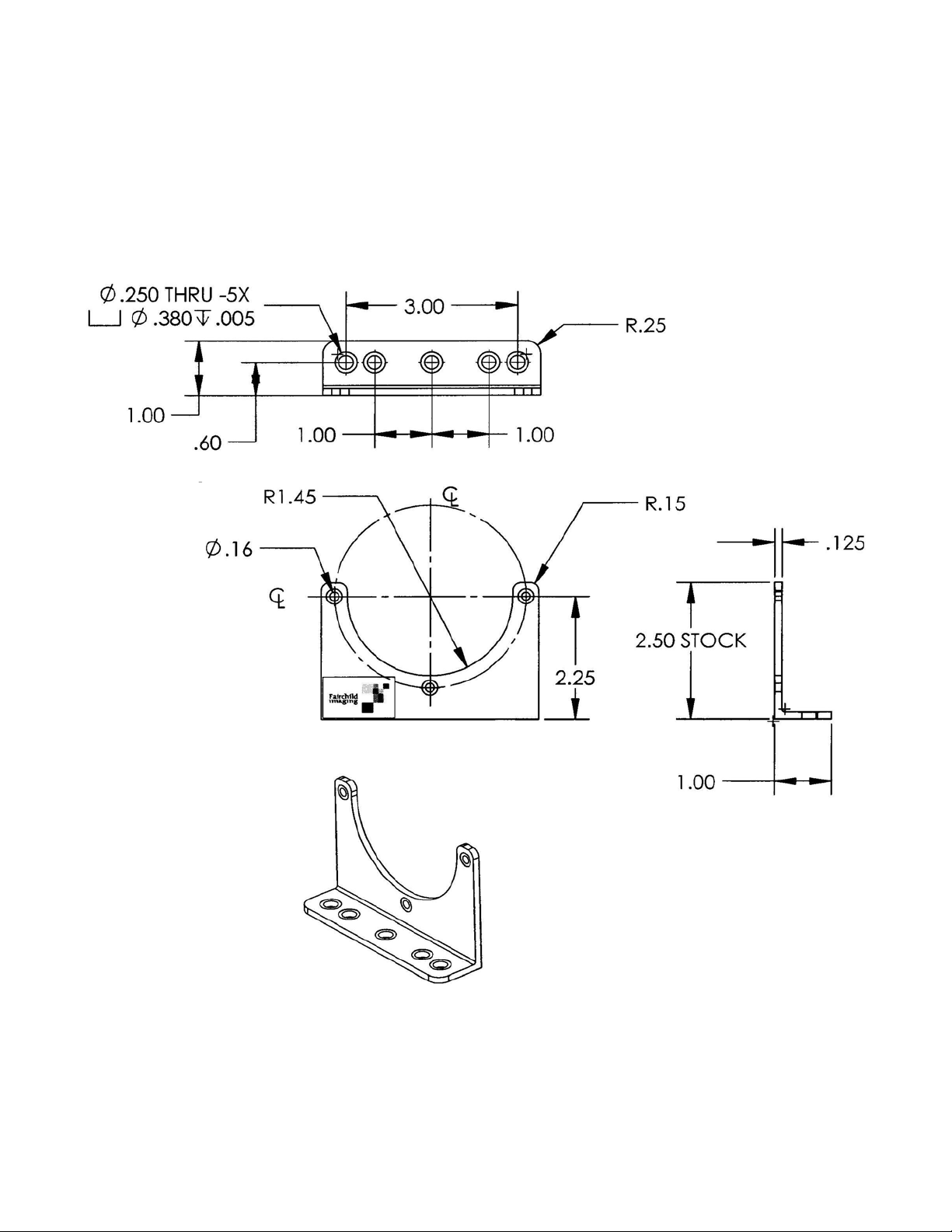
4.4 Mechanical Drawing of Available
Camera Face Mounting “L” Bracket
Contact your Fairchild Imaging representative for more details
Figure 4.4.1
Fairchild Imaging • CAM/CMOS-2K.LS Line Scan Camera User’s Manual • Rev C• 29 of 42
Page 30
4.5 Lenses
Fairchild Imaging does not supply lenses.
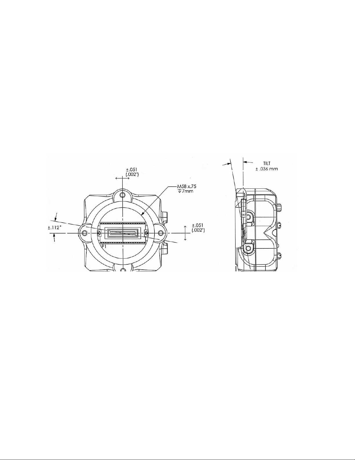
4.6 Positioning Accuracy of the Sensor Chip in the Camera
Positioning accuracy of the sensor chip in the horizontal and vertical direction is + 0.2 mm.
Rotational positioning accuracy is as shown. Reference position is the center of the camera
housing.
Since the translatory and rotational positioning tolerance depend on each other, the worse case of
maximum rotational and horizontal/vertical mis-positioning can not occur at the same time.
Figure 4.6.1
4.7 Illumination
In your application you must know the amount and wavelengths of light required. Some additional
things you want to consider respective to illumination are the characteristics of your light source
and the spectral characteristics and speed of the object(s) being inspected.
4.8 Light Sources
When selecting and setting up your light source you should be aware of the following.
• Light sources do age over time.
• When light sources age, they may produce less/more light in some areas of the spectrum.
Fairchild Imaging • CAM/CMOS-2K.LS Line Scan Camera User’s Manual • Rev C• 30 of 42
Page 31
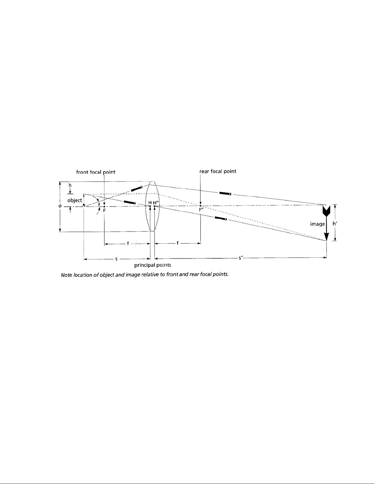
4.9 Lens Modeling
Several camera companies have included this and like information in their manuals. For reference
material it is very useful.
The focal point is the point at which the image of an infinitely distant object is brought to focus.
The effective focal length (f’) is the distance from the second principal point to the second focal
point. The back focal length (BFL) is the distance from the image side of the lens surface to the
second focal point. The object distance (OD) is the distance from the first principal point to the
object.
Figure 4.9.1
Fairchild Imaging • CAM/CMOS-2K.LS Line Scan Camera User’s Manual • Rev C• 31 of 42
Page 32

SECTION 5
Handling Instructions
5.1 Electrostatic Discharge
The Fairchild Imaging LNL2048S is a metal oxide semiconductor (MOS) device, and as all
such devices, has some limited inherent susceptibility to electrostatic discharge (ESD).
All reasonable and customary design steps have been taken to provide ESD protection
circuitry. The CMOS technology provides greater immunity to ESD problems than do CCD
devices.
Electrostatic charge placed at the sensor could cause charging of the chip which in
some situations might not be readily dissipated and minor impact on performance
might be temporarily experienced. Therefore, do not insert your finger or any other
object into the lens mount barrel.
5.2 Preventing ESD Damage
Please be certain to ground yourself prior to handing the camera.
Ensure that your working environment is grounded, including conductive floor mats.
Do not touch the window of the imager.
5.3 Protecting Against Dust, Oil and Scratches
Be certain to avoid dust buildup on the sensor window, where it could block the
optical path.
By not touching the surface of the sensor, you avoid introducing oil and avoid scratching the
sensor window. Again, you should not insert anything into the lens mount barrel.
5.4
Use compressed air to blow off particulate.
Cleaning the Sensor Window
If for some reason cleaning of the sensor window is required, use lens wiping cloth with a
small amount of eyeglass cleaning fluid. Do not use solvent as it may smear the sensor
window.
Fairchild Imaging • CAM/CMOS-2K.LS Line Scan Camera User’s Manual • Rev C• 32 of 42
Page 33

SECTION 6
Troubleshooting
6.1 Check the Obvious Things Out First
When trouble shooting, you want to start the process with the obvious components contained
within your system:
• Computer system: hardware & software
• Is the frame grabber plugged into the correct slot on the mother board
• Are all electrical connections secure
• Check to make sure that your light source is fully functional
• Make sure that the pin configurations for all of your cables are correct
• Make sure you have selected the correct lense for your camera
6.2 Use the Camera Control Interface to Perform Checks
In the Camera Control function, verify that the camera returns the control screen. Verify that you
can set various operating parameters.
6.3 Other Areas You Should Check
Contact Customer Support
Before you call for support, be sure to make a note of the camera settings and the frame grabber
settings you are using. You should also have saved captured live images. Customer support will
frequently request that you e-mail copies of these captured images. See Section 7.
Connections
Double check the pin outs of your cable. Make sure that the connections to the back of the camera
and to your PC are secure.
Power Supply Voltage
Make sure and measure that you have 5.0 volts at the camera connector.
Noisy Power Supply
Check your power supply voltage output(s). Check also the noise and ripple specification of your
power supply and measure both at the power supply output.
Fairchild Imaging • CAM/CMOS-2K.LS Line Scan Camera User’s Manual • Rev C• 33 of 42
Page 34

Everything Seems To Be Working, But No Image
Remove the cover from your PC and reset all the cards into the Mother board. Sometimes
when you move your PC, cards inside the PC work themselves loose.
Data Clocking/Output Signals
Verify the presence of all data clocking and output signals.
Horizontal Lines or Patterns in Output
To eliminate this type of problem use a DC light source.
No Output Or Non Specification Output
If your camera has no output or is putting out an unspecified signal unkown to you. Check the
length of your cable. If it is unnecessarily too long, and is also not shielded, your cable most likely
is picking up radiated noise and is inputting the noise into your camera.
Vertical Patterns in Output
Sometimes you might see patterns in your output. Most likely these are caused by dirt on
your lens or possibly contaminants on the sensor window. Clean both to remove all
contaminants.
Images are too Bright or too Dark
The causes to this problem should be obvious, but many times are overlooked. If your
image that you have captured is too dark or light, then experiment with the lens aperture.
Sometimes if you lengthen or shorten the exposure time this will effect your image.
Remember your camera control command “CPG”. This command allows you to either
increase or decrease pixel gain, which can have a dramatic impact on your image.
Lastly, don’t forget to check your lighting.
Images Look Noisy
There are several things that can cause this condition. Remember our camera command “CPG”.
Work with this command. Try increasing and decreasing pixel gain until you find the right setting.
Look for an increase in dark current. If the ambient temp. increases this will cause noise in the
image.
Look at your light source. If your light source is AC instead of DC this will make the image look
noisy. Also if the object you are inspecting has different surface textures this could produce an
image that may look noisy.
Bits That Do Not Change Value
If you see that data bits are not changing values, after you have changed them, then the first thing
to check is that the camera is not saturated by preventing light from entering. Next, disconnect the
Camera Link cable from the camera. Check the digital signals at the output of the camera,
ensuring that the correct values and signals are present.
Fairchild Imaging • CAM/CMOS-2K.LS Line Scan Camera User’s Manual • Rev C• 34 of 42
Page 35

SECTION 7
Product Support
If after troubleshooting your camera, and you still have problems, collect the following data about
your application and situation and call Fairchild Imaging Customer Support.
Note: You may want to photocopy this page to fax to Fairchild Imaging @ 408-735-7352
Your Name
Company name
Your phone number
Your Fax number
Product Model Number
(e.g. CAM/CMOS – 2K.LS)
Camera serial number
Detailed description of problem encountered
Please attach description with as much detail as
appropriate
When calling Fairchild Imaging, 1-800-325-6975, ask for Customer Support.
Fairchild Imaging • CAM/CMOS-2K.LS Line Scan Camera User’s Manual • Rev C• 35 of 42
Page 36

REFERENCE A
Camera Link
TM
Introduction
Camera Link is a Protocol that is Implemented in Channel Link Hardware
Camera Link is a communication interface for machine vision. The interface extends the underlying
technology of Channel Link to provide a specification more useful in this application.
For years, the scientific and industrial digital video market has lacked a standard method of
communication. Both frame grabbers and camera manufacturers developed products with different
connectors, making cable production difficult for manufacturers and very confusing for consumers.
A connectivity standard between digital cameras and frame grabbers has been long overdue and
will become even more necessary as data rates continue to increase.
Increasingly, diverse cameras and advanced signal and data transmissions have made a
connectivity standard like Camera Link a necessity. The Camera Link interface will reduce support
time, as well as the cost of that support. The standard cable will be able to handle the increased
signal speeds, and the cable assembly will allow customers to reduce their costs through volume
pricing.
Channel Link is a Widely-Used Signaling Method
National Semiconductor initially developed the Channel Link technology for flat-panel displays, and
based it on the LVDS physical layer. This technology was then extended for general-purpose data
transmission. Channel Link is built up of sets of driver and receiver pairs. Each driver set accepts 28
single-ended data signals and an accompanying single-ended clock. This data is serialized 7:1, and the
resulting four data streams and clock signal are driven over five LVDS pairs. The receiver accepts these
five signals and drives the full 28 bits and clock signal to its output pins as shown in Figure A.1.
Channel Link's transmission method requires fewer conductors to transfer data and allow for a smaller
connector, which is important for compact cameras such as the CAM/CMOS – 2K.LS
The Channel Link chipset provides data transmission rates up to 2.38 Gbit/sec.
Channel Link uses LVDS, a Low-Voltage Differential Signaling Standard
Low Voltage Differential Signaling (LVDS) is a high-speed, low-power general purpose interface
standard. The standard, known as ANSI/TIA/EIA-644, was approved in March 1996. LVDS uses
differential signaling, with a nominal signal swing of 350mV differential. The low signal swing decreases
rise and fall times to achieve a theoretical maximum transmission rate of 1.923 Gbps into a lossless
medium. The low signal swing also means that the standard is not dependent on a particular supply
voltage. LVDS uses current-mode drivers, which limit power consumption. The differential signals are
immune to up to ±1 V common volt noise.
Fairchild Imaging • CAM/CMOS-2K.LS Line Scan Camera User’s Manual • Rev C• 36 of 42
Page 37

Video Data Signals
The Channel Link technology is integral to the transmission of video data. Image data and image
enable signals are transmitted on the Channel Link bus. Four enable signals are:
FVAL-Frame Valid (FVAL) is defined HIGH for valid lines (not used by the
CAM/CMOS – 2K.LS).
LVAL-Line Valid (LVAL) is defined HIGH for valid pixels (LineValid Output in the
CAM CMOS – 2K.LS).
DVAL-Data Valid (DVAL) is defined HIGH when data is valid (Always High in the
CAM/CMOS – 2K.LS).
Spare- A spare has been defined for future use (not used by the CAM/CMOS–
2K.LS).
In the general specification, all four enable signals must be provided by the camera on each Channel
Link chip. All unused data bits must be tied to a known value by the camera.
For more information on image data bit allocations, refer to the official CameraLink
(http://www.machinevisiononline.org
.).
TM
specification
Camera Control Signals
Four LVDS pairs are reserved for general-purpose camera control. They are defined as camera inputs
and frame grabber outputs. Camera manufacturers can define these signals to meet their needs for a
particular product. In the case of the Fairchild Imaging CAM/CMOS - 2K.LS, the signals are:
• "ExSync" Line Synchonization Input (generically Camera Control 1, CC1)
• "
•
• Spare, unused (generically Camera Control 4, CC4)
ElectShutter" Exposure Control Input (generically Camera Control 2, CC2)
Spare, unused (generically Camera Control 3 ,CC3)
Communication
Two LVDS pairs have been allocated for asynchronous serial communication to and from the camera and
frame grabber. Cameras and frame grabbers should support at least 9600 baud. These signals are:
SerTFG Differential pair serial communications to the frame grabber.
SerTC Differential pair serial communications to the camera.
The serial interface will have the following characteristics: one start bit, one stop bit, no parity, and no
handshaking. It is recommended that frame grabber manufacturers supply both a user interface and a
software application programmming interface (API) for using the asynchronous serial communication port.
The user interface will consist of a terminal program with minimal capabilities of sending and receiving a
character string and sending a file of bytes. The software API will provide functions to enumerate boards and
send or receive a character string.
Fairchild Imaging • CAM/CMOS-2K.LS Line Scan Camera User’s Manual • Rev C• 37 of 42
Page 38

Power
Per the standard, power is not provided on the CameraLinkTM connector of the camera. Power is
supplied through the Hirose connector.
Port Assignments
See Tables 3.4.1 for the options of using the CAM/CMOS - 2K.LS with CameraLinkTM.
In CameraLinkTM, a port is defined as an 8-bit word as shown in Figure A.2. The least significant bit
(LSB) is bit 0 and the most significant bit (MSB) is bit 7. The full configuration CameraLink
TM
utilizes
eight ports, "A" through "H," although the CAM/CMOS - 2K.LS Model Camera only requires three,
again as shown in Figure A.2.
For More Information on CameraLink
TM
Refer to the Automated Imaging Association's website at:
http://www.machinevisiononline.org
Fairchild Imaging • CAM/CMOS-2K.LS Line Scan Camera User’s Manual • Rev C• 38 of 42
Page 39
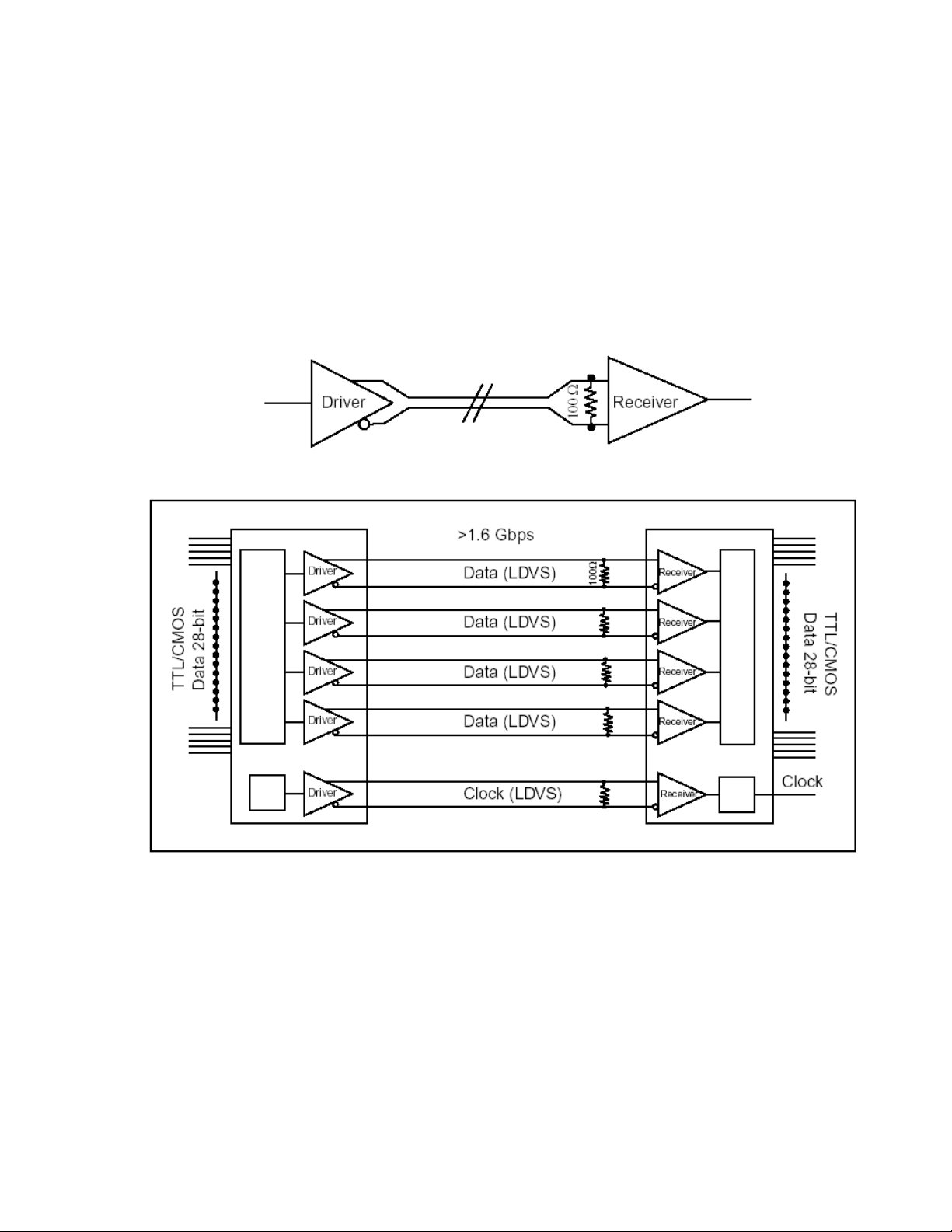
Camera Link Connections -- the MDR 26-Pin Connector
The 3M MDR-26 connector was selected for its robust design and reputation for success with highfrequency Channel Link transfer rates over several years of experience.
The MDR-26 connector is addressed in Section 2.2
Figure A.1
Channel Link Operation
Fairchild Imaging • CAM/CMOS-2K.LS Line Scan Camera User’s Manual • Rev C• 39 of 42
Page 40

Figure A.2
Data Routing for Base, Medium and Full Configurations
Fairchild Imaging • CAM/CMOS-2K.LS Line Scan Camera User’s Manual • Rev C• 40 of 42
Page 41
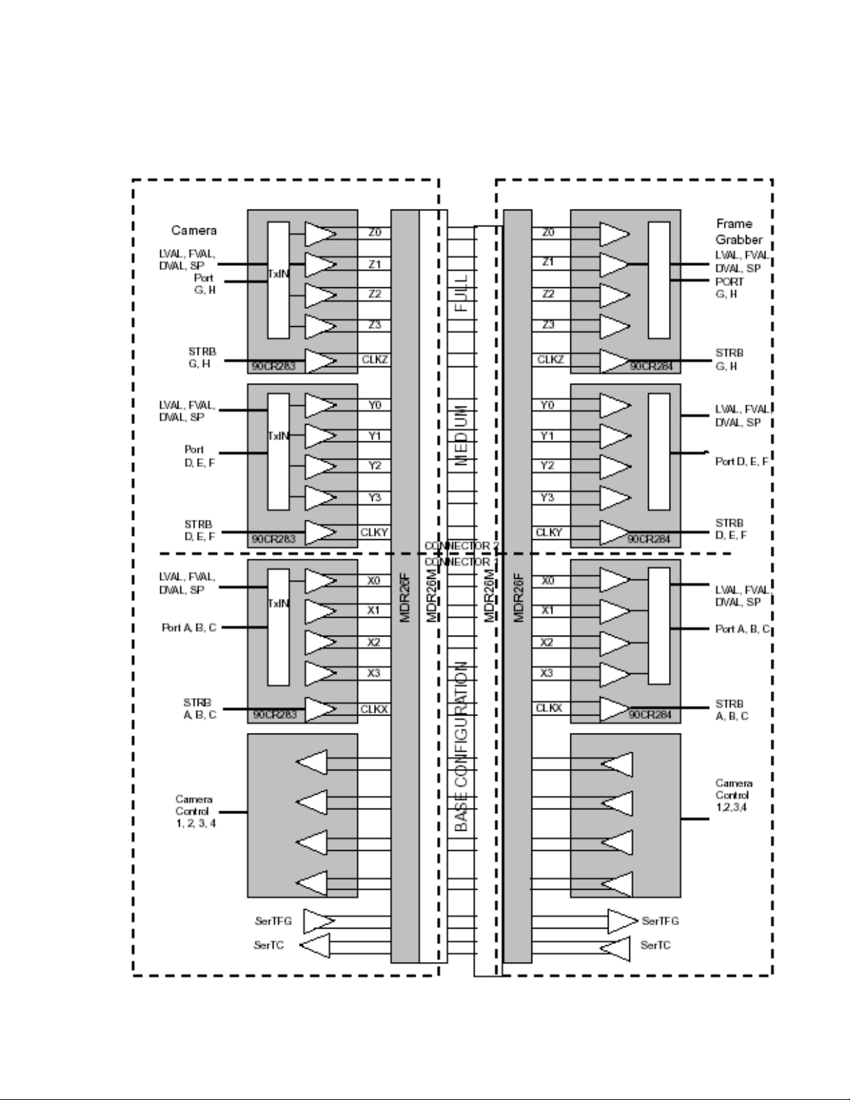
Figure A.3
Data Routing for Base, Medium and Full configurations
Fairchild Imaging • CAM/CMOS-2K.LS Line Scan Camera User’s Manual • Rev C• 41 of 42
Page 42
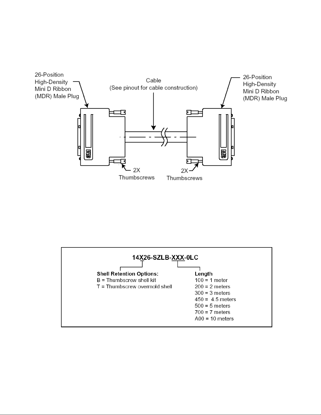
Figure A.4
Camera Link Cable
Figure A.5
3M Part Number Ordering Information
(see further www.3M.com)
Fairchild Imaging • CAM/CMOS-2K.LS Line Scan Camera User’s Manual • Rev C• 42 of 42
 Loading...